Power Supply Is The Foundation Of Electronic Equipment, And The Gate Driver Is The Key To Stably Providing Power To The Equipment. A Gate Driver Is A Power Amplifier That Accepts A Low Power Input From A Controller Chip And Generates A High Current Drive Input To The Gate Of A High Power Transistor Such As An IGBT Or Power MOSFET. This Article Will Introduce To You The Functional Characteristics, Electrical Parameters And Application Fields Of The Xinbolao Brand Gate Driver Chip Series, Gate Drive Power Supply Product Series.

01 —
Main Features
Latch Protection: Can Withstand 0.5A Reverse Current
Input Logic Protection Down To -10V
Low Output Impedance
Single Chip Integrates Two Channels Of Driver Output Peak Current: 2A
Working Range: 4.5V~25V
The Maximum Input Negative Voltage Can Reach -5V
High Capacitive Load Driving Capability: --At NF Load, Switching Time < 25ns
Rise/Fall Time Matching
Propagation Delay: 40ns
Wide Temperature Range: -40℃~125℃
Chip Turn-On/Turn-Off Delay Characteristics--Ton/Toff =70ns/70ns
Compliant With RoSH Standard SOIC8/DFN8
02 —
Functional Block Diagram (GT4426/GT4427/GT4428)

03 —
Package And Pin Definition (GT4426/GT4427/GT4428)

Serial Number | Name | Function |
1 | NC | Empty Pin |
2 | INA | Channel A Input |
3 | GND | Pin Ground |
4 | INB | Channel B Input |
5 | OUTB | Channel B Output |
6 | VCC _ | Power Supply |
7 | OUTB | Channel A Output |
8 | NC | Empty Pin |
04 —
Electrical Parameters (GT4426/GT4427/GT4428)
Symbol | Definition | Smallest | Maximum | Unit |
VCC _ | Voltage | 4.5 | 20 | V |
T C | Ambient Temperature | -40 | 125 | °C |
Symbol | Definition | Minimum Value | Typical Value | Maximum Value | Unit |
V I | Logic High “ 1 ” Input Voltage | 2.4 | V | ||
VIL _ | Logic Low “ 0 ” Input Voltage | — | — | 0.8 | V |
I IN | Input Current (0V≤ V IN ≤ V CC ) | 200 | ΜA | ||
V OH | High Level Output Voltage Drop | V CC –0.025 | — | — | V |
V OL | Low Level Output Voltage Drop | — | — | 0.025 | V |
R OH | High State, Output Resistance ( V CC = 18V, I O = 100 MA ) | — | 4 | 8 | Ω |
R OL | Low Level State, Output Resistance ( V CC = 18V, I O = 100 MA ) | — | 2 | 4 | Ω |
PK _ | Peak Output Current | 2 | A | ||
I REV | Latch Protection Can Withstand Reverse Current ( Duty Cycle ≤ 2%, T ≤ 300 Us , V CC = 18V) | — | >0.5 | — | A |
T _ | Rise Time ( V CC = 18V, C LOAD = 100 PF ) | — | — | 30 | Ns |
F _ | Fall Time ( V CC = 18V, C LOAD = 100 PF ) | — | — | 30 | Ns |
T ON | Turn-On Propagation Delay ( V CC = 18V, C LOAD = 100 PF ) | — | — | 70 | Ns |
T OFF | Shutdown Propagation Delay ( V CC = 18V, C LOAD = 100 PF ) | — | — | 70 | Ns |
I Q1 | Supply Current ( V INA = V INB = Logic High ) | — | — | 1 | MA |
I Q0 | Supply Current ( V INA = V INB = Logic Low ) | — | — | 1 | MA |
1. Model Selection And Input/Output Logic Comparison Table
GT4426 Input And Output Logic Table
INPUT | OUTPUT | ||
INA | INB | OUTA / | OUTB / |
L | L | H | H |
H | H | L | L |
L | H | H | L |
H | L | L | H |
Note: H Represents High Level; L Represents Low Level | |||
GT4427 Input And Output Logic Table
INPUT | OUTPUT | ||
L | L | L | L |
H | H | H | H |
L | H | L | H |
H | L | H | L |
Note: H Represents High Level; L Represents Low Level | |||
GT4428 Input And Output Logic Table
INPUT | OUTPUT | ||
INA | INB | OUTA | OUTB |
L | L | L | L |
H | H | H | H |
L | H | L | H |
H | L | H | L |
Note: H Represents High Level; L Represents Low Level | |||
Model | Input And Output Logic | Encapsulation |
GT4426 | Reverse Phase | SOP-8 |
GT4427 | In Phase | SOP-8 |
GT4428 | Channel A Is Inverted And Channel B Is In Phase. | SOP-8 |
2. Input And Output Waveforms Of Three Models Of GT4426/GT4427/GT4428

GT4426 Input And Output (Inverting) Waveform Diagram

GT4427 Input And Output (Non-Phase) Waveform Diagram

GT4428 Input And Output (A Channel Inverted) Waveform Diagram

GT4428 Input And Output (B Channel In-Phase) Waveform Diagram
05 —
Application Areas And Products
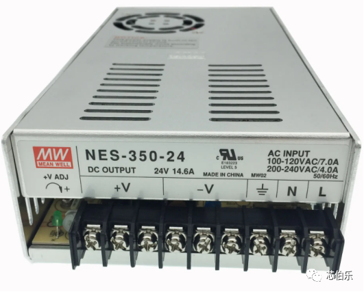
Conversion Power Supply

Pulse Generator
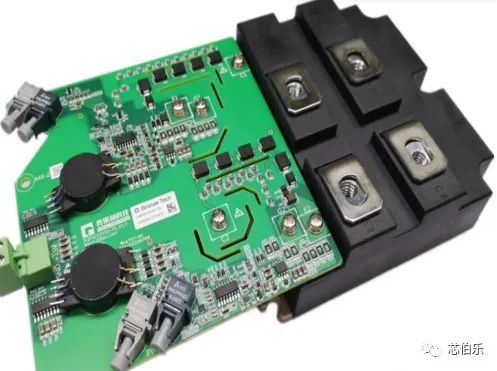
Application Of XBLW GT4428 Driving IGBT
06 —
Summarize
In Various Power Conversion Processes, Gate Drivers Play An Important Role, And Isolated DC-DC Converters That Drive Power Through The Gate And Support Bipolar Voltage Output Are Ideal For Providing Stable Power For Various Electrical Equipment. Choose. Xinbolao Has Launched A Series Of Isolated DC-DC Converters, Providing Product Series That Support Different Technologies Such As IGBT, MOSFET, SiC MOSFET And GaN, Which Can Meet The Different Power Requirements Of Various Applications. The Product Series Is Quite Complete And Will Be Your The Perfect Partner For Product Development.
Shenzhen Xinbol Electronics Co., Ltd. Is An Enterprise Specializing In The Research, Development And Sales Of Semiconductor Devices. Products Focus On Consumer And Industrial Markets. The Main Products Include Power Management IC, Low-Power LDO, Three-Terminal Voltage Regulator, High, Medium And Low Voltage MOS Tubes, Motor Driver, Interface RS485/RS232, Darlington And Logic Circuits , Etc.
Products Are Widely Used In Drones, Robots, Power Supplies, Computers, Instrumentation, Toys, Home Appliances, Communication Equipment, Lighting Applications, Automotive Electronics, Industrial Automation Equipment And Other Fields. Xinbolao Is Actively Committed To The Sustainable Development Of The Semiconductor Industry, Using Its Professional Experience In The High-Tech Field To Provide Excellent Quality Products And System Solutions To Build A Harmonious And Efficient Society, And Achieve A Win-Win Situation For The Entire Industry Chain.
Xinbolex XBLW Is The Independent Brand Of Xinbolei Electronics.
Recommend News
-
Phone
400-9682 003

