
XBLW 1A Low‑Dropout Linear Regulator XBL1117:High‑Precision & High‑Reliability Power‑Supply Solution
In various electronic devices, the stability and efficiency of power‑supply management directly determine overall system performance and reliability. Whether for industrial‑control equipment, network‑communication systems or consumer‑grade electronic products, requirements for power‑management ICs keep rising: not only high‑precision output and large‑current driving capability, but also low power consumption, high reliability and excellent temperature characteristics. XBLW’s XBL1117 series low‑dropout linear regulators, featuring 1A output current, ±1.5% output‑voltage accuracy and dropout voltage as low as 1.26V dropout characteristic, have become a preferred component for power‑supply design among numerous engineers.
1. Product Overview
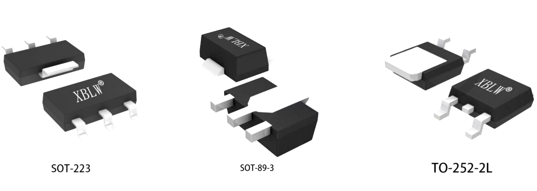
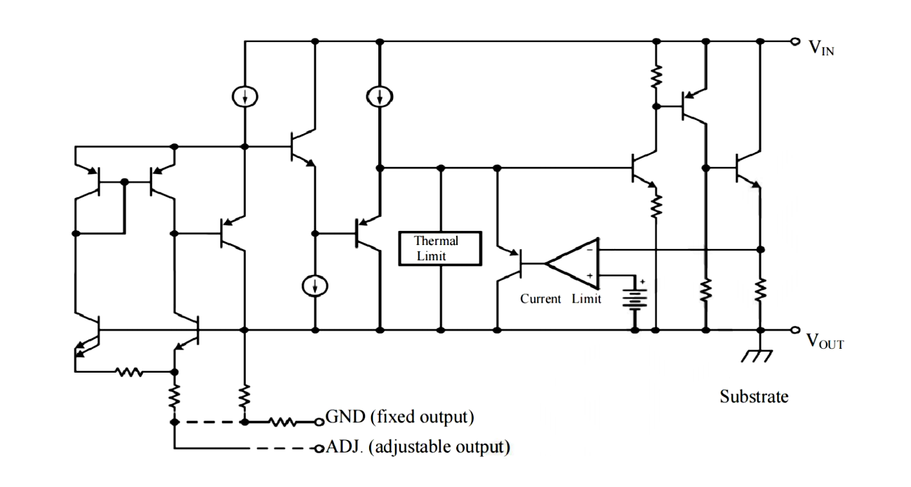
XBL1117 is a high‑precision low‑dropout linear regulator, offered in fixed‑output (1.2V/2.5V/3.3V/5.0V) and adjustable‑output (1.25V ~ 13.8V) versions, with ±1.5% output‑voltage accuracy. It integrates over‑current and thermal‑shutdown (125°C) protection. Maximum input voltage is 15V, operating temperature range: ‑40°C to +125°C. Three package options are available: SOT‑223, SOT‑89‑3L and TO‑252‑2L, targeting medium‑power, space‑constrained and high‑current applications respectively to meet diverse application‑scenario requirements.
2. Detailed Key‑Feature Description
l 1. High Output‑Current Capability
XBL1117 delivers continuous 1A output current with peak‑current capability up to 1.4A. This feature enables it to supply stable power for most medium‑power loads. Compared with competing products on the market, XBL1117 maintains excellent voltage‑regulation performance under full‑load conditions without large output‑voltage fluctuations caused by load variations.
l 2. Excellent Low‑Dropout Performance
Dropout voltage is a key parameter for evaluating LDO performance. A lower value means lower voltage‑drop loss between input and output, which not only optimizes overall power‑supply efficiency but also reduces thermal‑design requirements and helps control system heat‑dissipation cost and form‑factor size.
l 3. High Precision & Stability
XBL1117 achieves voltage accuracy up to ±1.5% and temperature stability better than 0.5%. Its line‑regulation is less than 0.2% over input‑voltage variations. These specifications guarantee that the output voltage remains highly stable under diverse operating‑condition and delivers reliable power for precision analog circuits and digital systems.
3. Typical Application Scenarios
l Network‑Communication Equipment
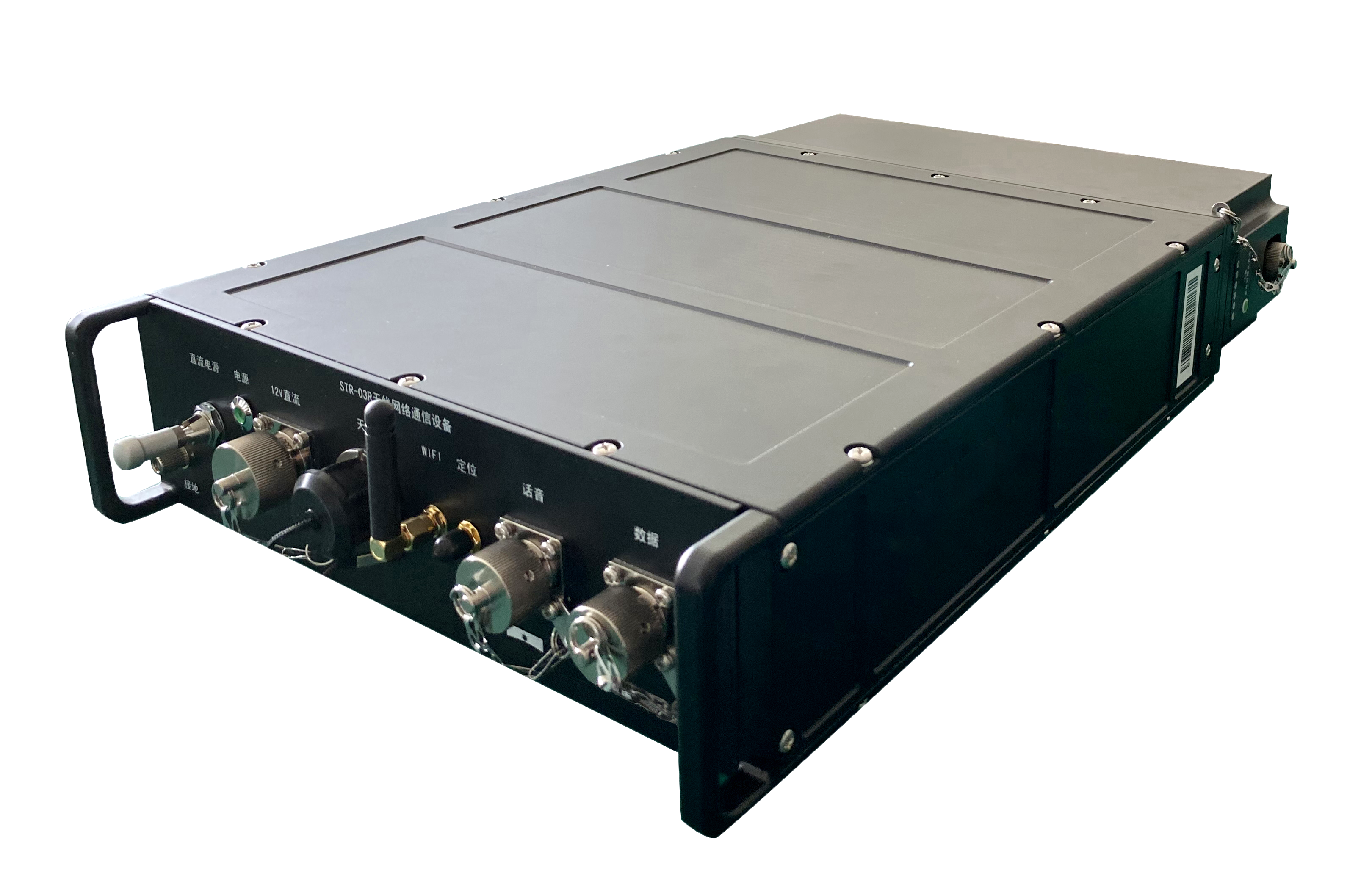
For communication equipment such as network switches and server power‑supply modules, XBL1117 is used for secondary voltage regulation to supply clean power for various interface ICs and processors. Its wide input‑voltage range (max. 15V) enables compatibility with different power adapters, while good ripple‑rejection performance helps reduce the impact of digital noise on analog circuits.
l Computers & Peripheral Devices
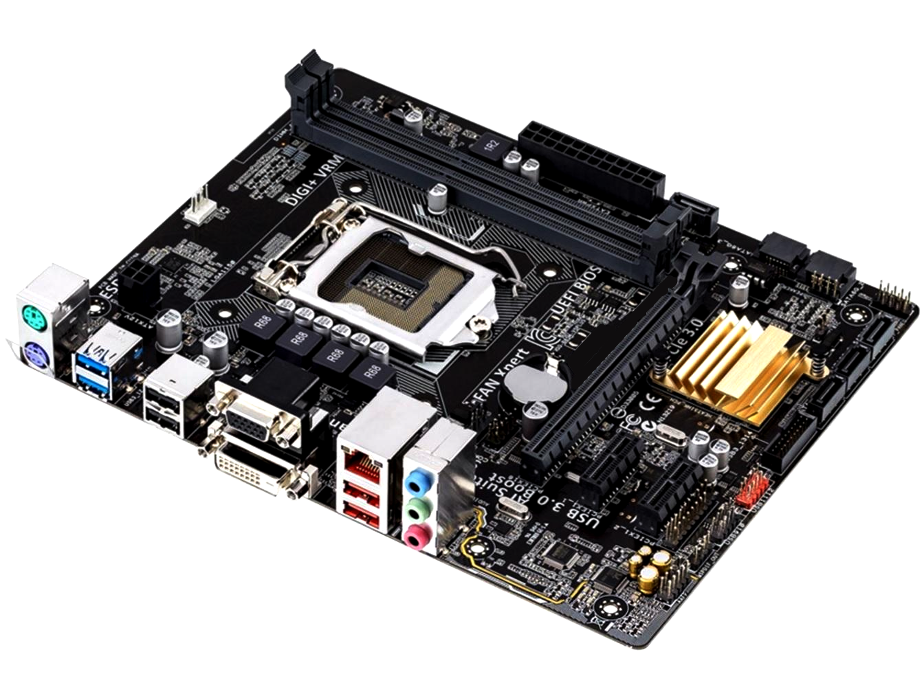
In computer motherboards, graphics cards and other devices, XBL1117 can be used for power supply of memory, chipset and other circuits. Its fast transient‑response characteristic meets dynamic‑load‑change requirements of processors, and low‑dropout performance helps reduce overall power consumption.
l Battery‑Powered Equipment
In battery‑powered devices such as portable instruments and IoT terminals, the low quiescent current and low‑dropout characteristics of XBL1117 help prolong battery service life. When used together with a DC‑DC converter, it forms an efficient and stable power‑supply system.

4. Typical Application‑Circuit Design Guidelines
1. Fixed‑Output Version Application
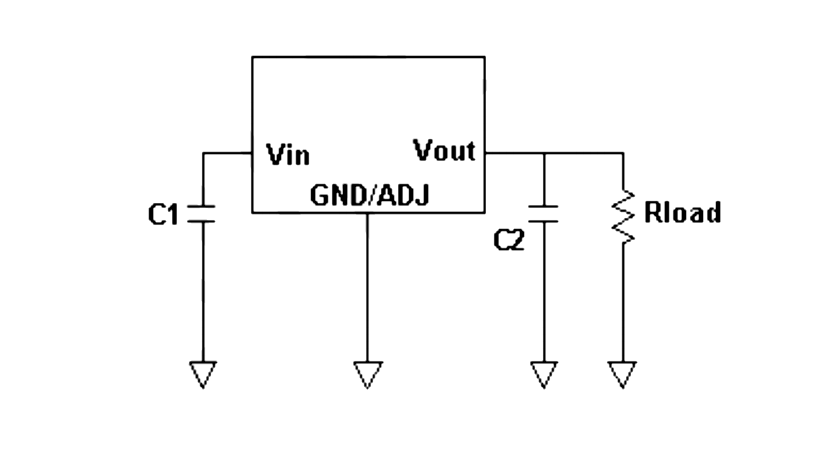
The application circuit of fixed‑output XBL1117 is extremely simple: it only requires one capacitor at the input terminal and one capacitor at the output terminal for normal operation. A 10μF tantalum or electrolytic capacitor is recommended as the input bypass capacitor, and a 22μF tantalum capacitor is used on the output side to guarantee stability. This simple peripheral‑circuit design greatly reduces system complexity and BOM cost.
2. Adjustable‑Output Version Application
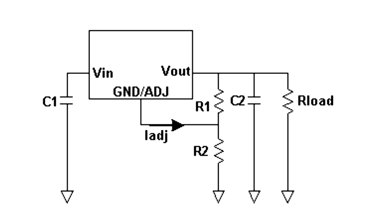
The adjustable‑output version sets output voltage via two external resistors. The formula is shown below:
VOUT = VREF * (1 + R2 / R1) + IADJ * R2
Where: reference voltage VREF=1.25V, adjust‑pin current IADJ ≈ 50μA, which can generally be ignored. For optimal performance, it is recommended to set R1 between 200Ω and 350Ω. Under this condition, current flowing through R1 is approximately 4‑6mA, which ensures no‑load stability without excessive power dissipation.
To improve ripple‑rejection ratio, connect a 10μF bypass capacitor CADJ between the adjust pin and GND. The impedance of this capacitor shall be lower than the resistance value of R1 to prevent ripple amplification at any ripple frequency.
5. Advantages vs. Competing Products
Compared with overseas competing products, XBL1117 delivers equivalent performance with obvious cost advantages. Its ±1.5% output‑voltage accuracy matches the performance level of international mainstream IC vendors at a more competitive price. Furthermore, XBLW provides comprehensive technical support and sample service to shorten customer development cycles. When compared with traditional three‑terminal regulators (e.g. 78‑series), XBL1117 features significantly better dropout‑voltage performance.
6. Summary
XBLW XBL1117 series low‑dropout linear regulators, featuring high precision, large output current, low power consumption and full‑featured protection functions, serve as an ideal choice for industrial and consumer power‑supply designs. Flexible package and voltage‑configuration options can satisfy diversified power‑management requirements. Whether deployed in network‑communication equipment, industrial‑control systems or consumer‑grade electronics, XBL1117 delivers stable and reliable power‑supply solutions and helps customers improve system performance and optimize overall system cost.
Recommend News


Follow Us


-
Phone
400-9682 003