
I. Chip Overview
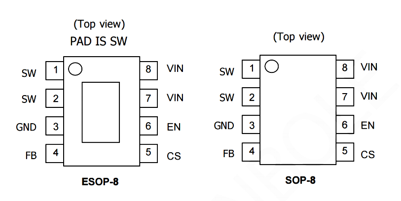
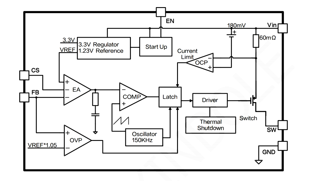
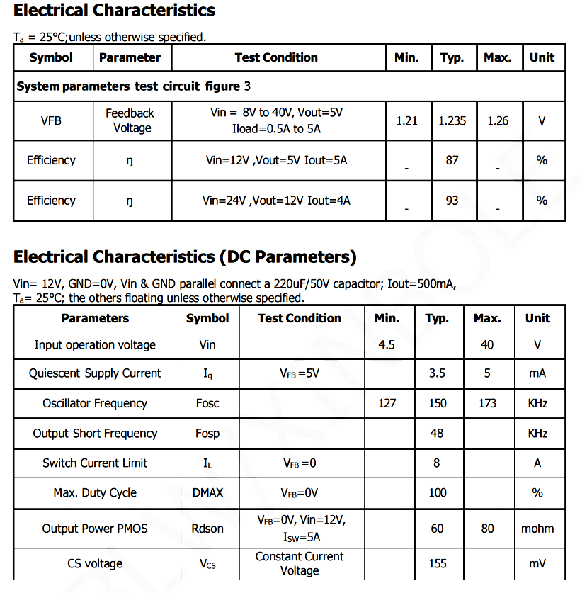
XBLW-XBL4001is abuck DC converterwitha wide input voltage range of 4.5V~40Vand an adjustable output voltage range between1.235V~37V. Its fixedswitching frequencyis150kHz, with a maximumoutput currentof5A (ESOP-8 package). The chip usesvoltage-mode asynchronous PWMcontrol, featuresON/OFF shutdown control, and can be started and stopped by logic level control.
II.Performance Features
01 丨 Wide Input Voltage
XBLW-XBL4001 4.5V~40Vwide input voltagerangecan adapt to various power supply input scenarios. It handles complex circuit environments and provides stable power support for various sensors, controllers, etc.
02 丨 Adjustable output voltage
03 | Built-in MOSFET
XBLW-XBL4001integratesMOSFETs,simplifyingcircuit designandreducingthe use of peripheral components. When used, only a small number of peripheral components are required for normal operation. This not only improvesthe system's integrationand reliability, but also savesengineers valuable
04 丨 Low-power standby mode
XBLW-XBL4001featuresa low-power standby modethat effectively improves system energy efficiency. In standby mode, the chip's power consumptionstatic currentis only3.5mAwhich is particularly important for devices that need to run for a long time, effectively extending the device's life
III.Protection Features and Control Characteristics
01 丨 Over-temperature protection
XBLW-XBL4001 is equipped withover-temperature protectionfunction, which can monitor the chip temperature in real-time. When the temperature is too high, the chip will automaticallyshut down the output,avoidingchip damagecaused byoverheating, ensuring the safe operation of the device under extreme conditions.
02 丨 Overcurrent Protection
XBLW-XBL4001featuresovercurrent protectionfunction, which canprecisely limit the output current.It canpreventfailurescaused by the overload or short circuit of downstream devicesandprovidesstableandsafe protectionfor the chip and the entire system.
03 丨 Disable control function
XBLW-XBL4001hasa shutdown control function, which can becontrolled bylogic levelto output start/stop. When in use, it is sufficient to connect the chip's EN pin tohigh level or floatingtoenable the output (high open, low close).
IV.Typical Application Circuits
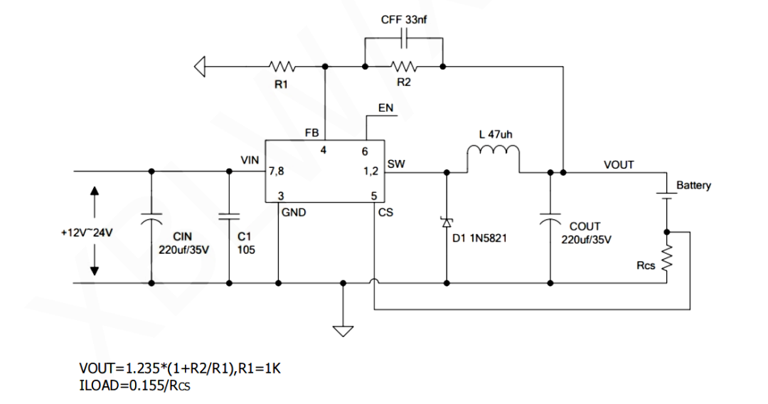
5V/5A output circuit
XBLW-XBL4001When outputting5V/5Acurrent, the peripheral circuit design is relatively simple. According to the formulaUout=1.235*(1+R2/R1), when R1=1KΩ, R2=3KΩ is sufficient to obtain an output voltage of 5V.
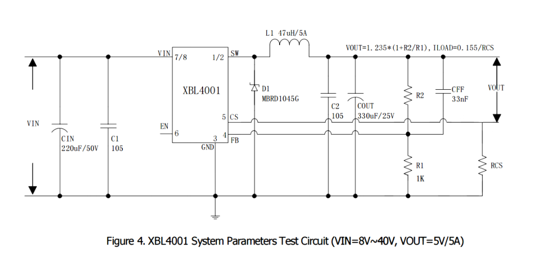
12V/4A output circuit
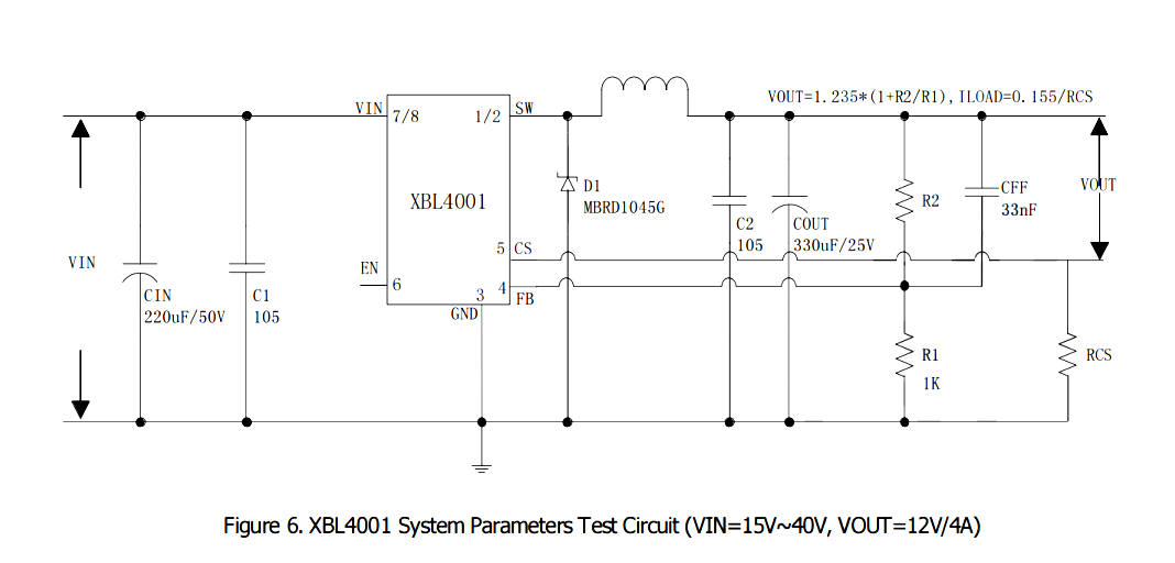
XBLW-XBL4001When outputting12V/4A, according to the formulaUout=1.235*(1+R2/R1), when R1=1KΩ, R2=8.7KΩ will yield an output voltage of 12V.
Standby mode control circuit
XBLW-XBL4001 standby mode control circuit can control the chip output via logic level control. The logic for the EN pin of XBLW-XBL4001 is high or floating to enable the output and low to disable the output (i.e., high-open, low-close). When in use, it is sufficient to connect the corresponding logic level to the sixth pin (EN pin) of XBL4001 to enable the output.
V. Packaging Form
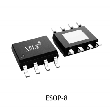
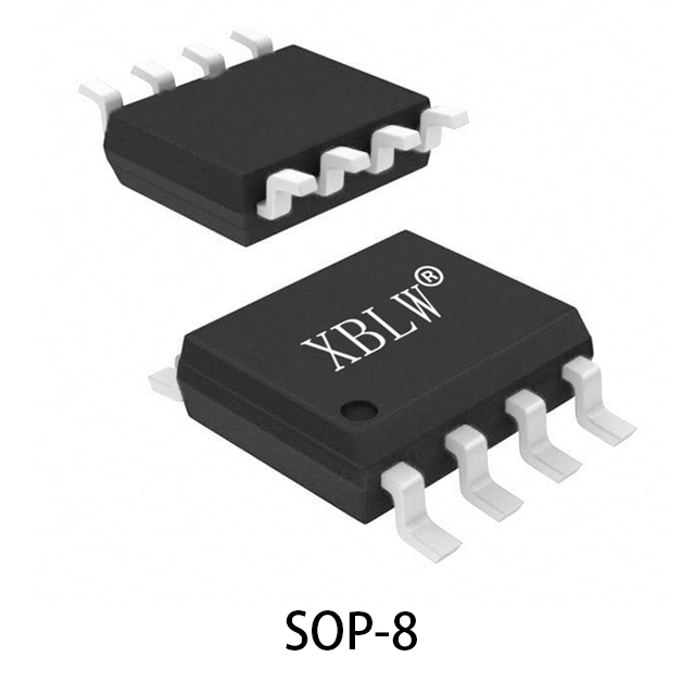
XBLW-XBL4001providestwo package types:SOP-8andESOP-8.The SOP-8 packagehas a maximumload current of 2Aand is suitable for circuits with general low current requirements.The ESOP-8package isbased onSOP-8andoptimizesheat dissipation performancecompared tothe SOP-8packagewith a loadcapacity increased to5Aand is suitable for high power density designs, effectively improving the chip's heat dissipation efficiency and extending its service life.
VI. Electrical Performance Parameters
VII.Absolute Maximum Ratings and Operating Conditions
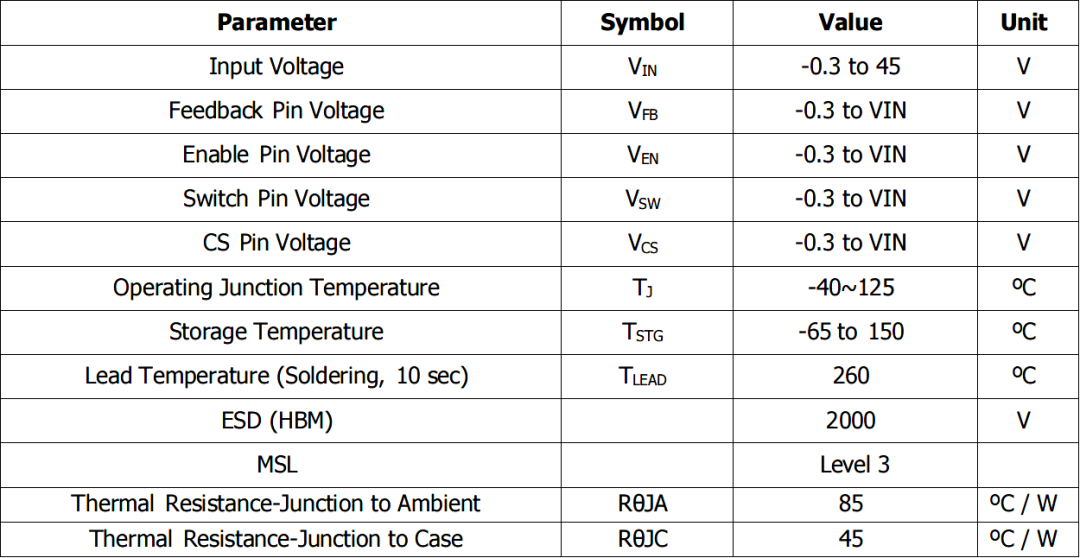
Note: Exceeding the maximum rated stress may cause permanent damage to the equipment. Please note that this only indicates the stress level and does not mean that the equipment will continue to operate normally under these or other conditions at or above the indicated values. Prolonged exposure to absolute maximum rated values may adversely affect the reliability of the equipment and should be avoided as much as possible during use.
VIII. Conclusion
Recommend News


Follow Us


-
Phone
400-9682 003