
In the field of electronic engineering, precise current measurement is crucial for numerous circuit designs and system monitoring. The XBLW GT712 current sensor, launched by XBLW, has become the preferred tool for engineers in many applications due to its unique advantages. This article will delve into the working principle, performance characteristics, and key application points of the XBLW GT712, providing engineers with detailed and professional reference information to help them better understand and utilize this critical component.
I. Working Principle Analysis
The XBLW GT712 is designed based on the Hall effect principle. When the measured current flows through the wire inside the sensor, it generates a magnetic field around it. The Hall element in the sensor is placed in this magnetic field. According to the Hall effect, the magnetic field acts on the semiconductor material of the Hall element, causing the charge carriers within the material to deflect, which in turn generates a Hall voltage at the output terminal of the Hall element. This voltage is closely related to the magnetic field strength, and the magnetic field strength is linearly related to the measured current, thereby achieving an accurate measurement of the current magnitude.
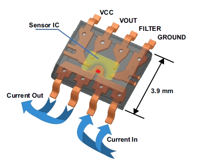
To enhance the magnetic induction effect and ensure measurement accuracy, the XBLW GT712 uses a magnetic core made of magnetic material internally. The current-carrying wire passes through the air gap of the magnetic core, which concentrates and guides the magnetic field near the Hall element, allowing the Hall element to detect magnetic field changes more efficiently and thereby improving measurement sensitivity. At the same time, the sensor also integrates a signal processing circuit to amplify, filter, and modulate the weak voltage signal generated by the Hall element, making its output voltage signal more stable and accurate, which is more suitable for subsequent circuit reading and processing.
II. Pin Introduction and Usage
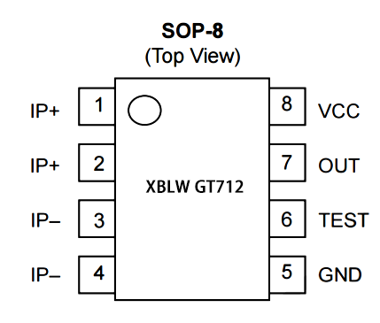
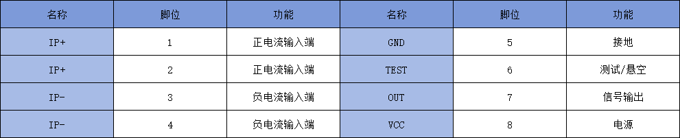
The main pins of the XBLW GT712 include
Test current input and output terminals (IP+, IP-)
Ground (GND)
Power supply end (VCC)
Output voltage terminal (VOUT)
When in use, IP+ and IP- are connected to the positive and negative terminals of the measured current, GND is grounded, VCC is connected to a 5V power supply, and VOUT is connected to the analog input pin of the ADC acquisition chip to read the voltage signal. The XBLW GT712 uses the Hall effect to achieve non-contact current detection, with an isolation voltage of up to 2500V. It calculates the current value by measuring the output voltage and based on the chip's sensitivity and zero-point voltage. When no current flows through the chip internally and it is powered by 5V, the GT712 outputs a zero-point voltage of 1/2VCC, which is 2.5V. Based on this, for every 1A increase in current, the corresponding output voltage increases by 185mV/100mV/66.7mV (depending on the different range versions).
III. Performance Characteristics
01
Multiple range selection:
The XBLW GT712 offers models with different ranges such as 5A, 20A, and 30A, meeting the diverse needs of engineers in various applications. With multiple sensitivity options including 185mV/A, 100mV/A, and 66.7mV/A, it can be precisely matched for low-current detection in small electronic devices as well as larger current monitoring in industrial power systems, ensuring a wide and accurate measurement range.
02
High linearity:
Its output voltage exhibits an excellent linear relationship with the measured current, with a linearity error of only 0.4%. The linearity error is extremely small across the entire range, allowing it to accurately reflect the actual changes in current. This provides a solid guarantee of data accuracy for engineers in circuit design and analysis, making the current measurement results more reliable and facilitating subsequent circuit debugging and optimization.
03
Rapid response capability:
It features a fast response speed with a typical response time of 4us, enabling it to react accurately to current changes in a short period of time. It ensures real-time monitoring of rapid current fluctuations, promptly detects and handles abnormal situations in the circuit, and ensures stable system operation. The 120kHz bandwidth also allows the XBLW GT712 to capture and respond to higher-frequency current changes.
04
Excellent isolation properties:
It achieves a high degree of isolation between the primary circuit (the circuit under test) and the secondary circuit (the signal output circuit), with an isolation voltage as high as 2500V. This effectively avoids interference from high-voltage and high-current circuits on the signal processing circuit, ensuring the safety and stability of the measurement system, and eliminating concerns about mutual interference during the signal transmission process.
IV. Typical Principle Diagrams and Applications
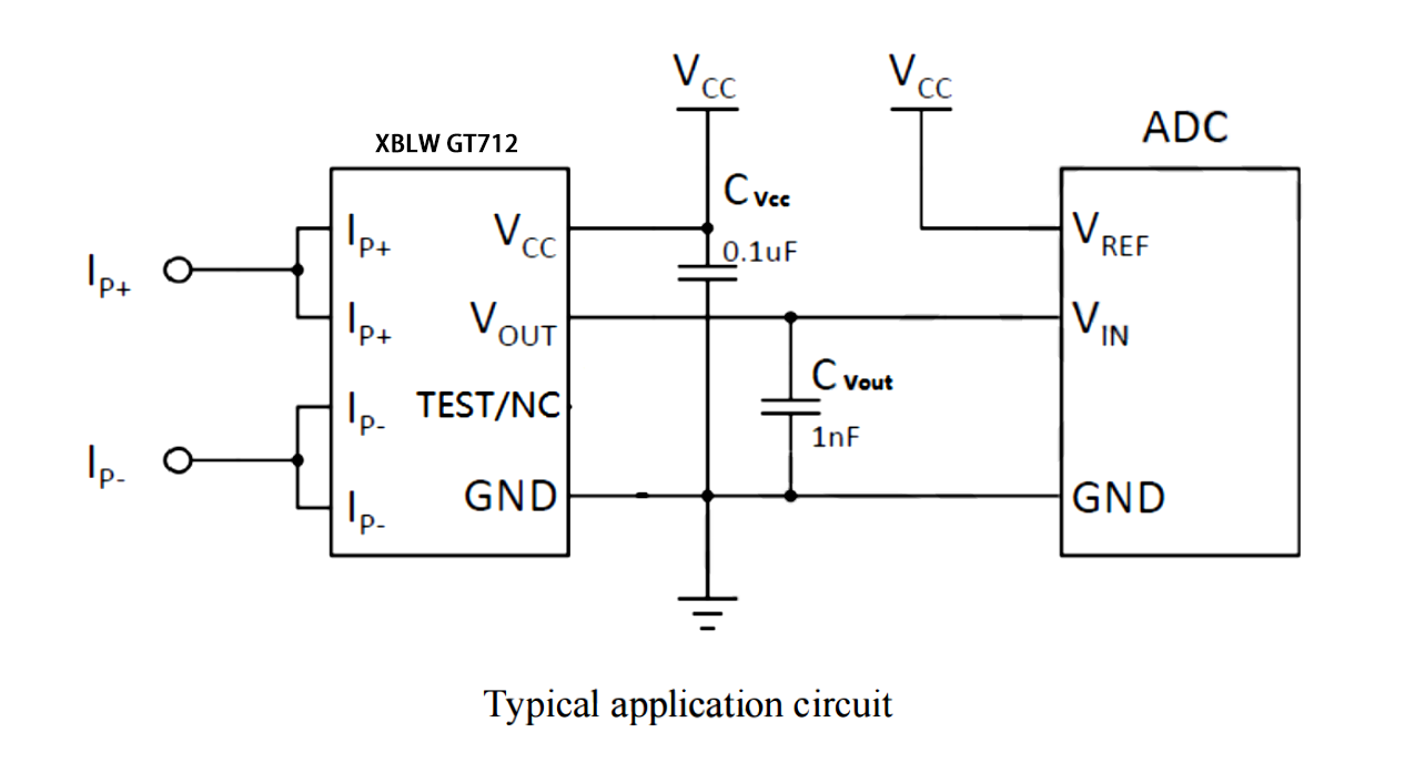
The typical application circuit of the XBLW GT712 requires a filter capacitor CVcc between VCC and GND, and an additional filter capacitor CVout between the output and GND. At the input end of the measured current, pins 1 and 2 are shorted together to serve as the input end of the measured current, while pins 3 and 4 are shorted together to serve as the output end of the measured current. The sensor's analog output signal is directly proportional to the measured AC/DC current.
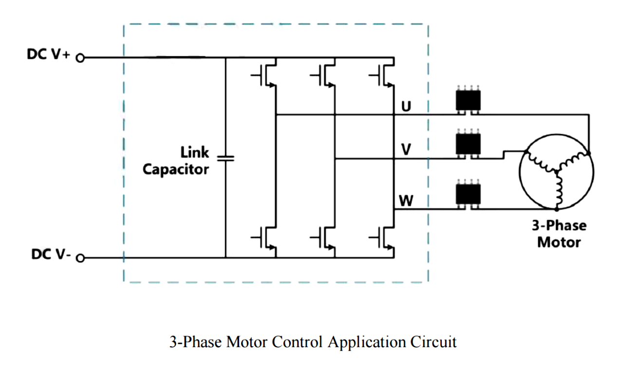
The figure shows a three-phase motor current detection circuit based on the XBLW GT712. By placing the XBLW GT712 in series with the branch whose current needs to be measured, and using an external ADC to acquire the output voltage, the current value can be accurately read, enabling precise motor control and overcurrent protection to prevent the motor from being damaged by excessive current.
In actual customer use, the ADC sampling chip selected by the customer may fail to capture the maximum voltage of 4.5V (full-scale maximum output voltage). In this case, a voltage divider can be used to reduce the voltage to a measurable range, but it needs to be calculated in conjunction with an algorithm. The circuit is shown as follows:
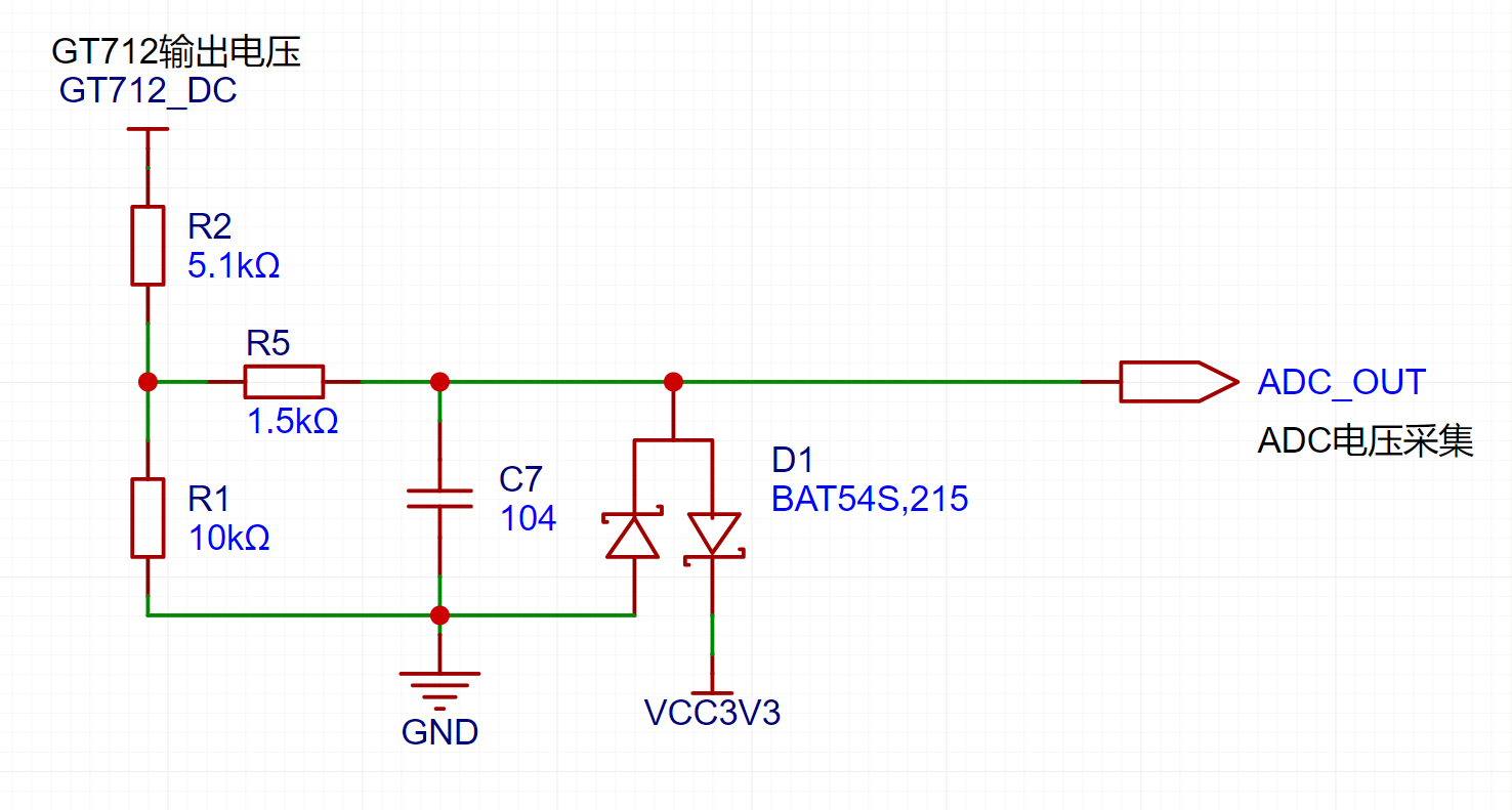
At this time, the voltage collected by ADC_OUT is ADC_OUT = GT712_DC * R2 / ( R1+R2 ) = GT712_DC * 0.34. At this time, the voltage is 0.34 times the original voltage, meeting the voltage requirement of 3.3V for the ADC sampling chip. When calculating the current, the sampling current = (GT712_DC - 0.5VCC) / Sensitivity = [(ADC_OUT / 0.34) - 0.5VCC] / Sensitivity.
The D1 diode is a clamping diode that prevents unexpected high voltages from entering the detection circuit and burning out the downstream circuit. When a negative voltage is present, the diode on the left side is turned on, clamping the voltage to -0.3V. When an unexpected positive high voltage enters, the diode on the right side, combined with the R5 resistor, forms a clamping circuit, clamping the voltage to 3.3+0.3V, with the excess voltage being handled by R5. The selection of the voltage divider resistor requires choosing an appropriate precision based on the project's specific requirements.
V. Other Customer Questions
1
When a chip is used to measure the current on a three-phase motor, will the current exceed the chip's range at the moment of startup and damage the chip?
Answer: No, this was already taken into account during the development and design of the XBLW GT712, and the chip can withstand a maximum surge current of 100A.
2
Are chips directly connected in series into the circuit?
Answer: Yes, you just need to connect P+ and P- in series into the circuit like measuring current with an ammeter, and then power the GT712 chip, and it will output voltage normally.
3
How to convert the voltage after GT712 output into current.
Answer: The output voltage needs to be acquired by an ADC, and the current can be calculated from the acquired voltage using the formula (GT712_DC - 0.5VCC) / Sensitivity (where GT712_DC is the output voltage of the GT712).
4
The GT712 output voltage is a maximum of around 4.5V at full scale, but the ADC can only collect a maximum of 3.3V. What should I do?
Answer: After collecting the voltage after dividing it using a resistor, the current value is finally calculated using a formula algorithm. Pay attention to the selection of resistor accuracy; for details, please refer to the typical schematic diagram and application in the text above.
VI. Application Key Points Guide
01
Circuit layout optimization:
When designing the circuit board, the XBLW GT712 should be placed as close as possible to the source of the measured current to minimize wire length, thereby reducing the impact of line impedance and induced noise on the measurement results. At the same time, pay attention to the routing of the signal output lines, avoiding parallelism or crossing with high-current and high-voltage lines to reduce electromagnetic interference and ensure the purity of the output signal, providing high-quality raw data for subsequent signal processing.
02
Application of filtering processing:
Due to the complex actual circuit environment, various electromagnetic interferences may exist, causing noise to be mixed into the XBLW GT712 output signal. Engineers can connect appropriate filtering circuits, such as low-pass filters, to the sensor's output end, select suitable filtering parameters based on specific application scenarios, filter out high-frequency noise signals, and improve the accuracy of the measurement data.
03
Notes:
Since the Hall element is located at the bottom center of the chip, this area of the chip should be avoided as much as possible for routing and signal interference. To better prevent external interference, it is recommended to add a surface-mount magnetic alloy shield to the device package. At the same time, to ensure the effectiveness of the shielding without affecting the pin connections, an appropriate space should be left for the shielding layer near the integrated circuit pins. This way, the external magnetic field interference on the Hall element can be minimized to the greatest extent possible without interfering with normal connections.
In the field of electronic engineering, precise current monitoring and control technology has always been the key to improving system performance and reliability. The XBLW GT712 current sensor from Sino-Bole, with its excellent performance and exquisite design, provides engineers with a powerful tool that not only enhances measurement accuracy but also simplifies the complexity of system design. With its high bandwidth, fast response time, and excellent linearity, the GT712 ensures the real-time accuracy of current monitoring, offering great convenience to engineers in their designs. This not only helps promote the development of the electronic engineering field but also provides engineers with more opportunities to achieve technological breakthroughs.
Recommend News

Follow Us


-
Phone
400-9682 003