
Article Introduction:
In today's digital age, POE (Power over Ethernet) devices are widely used because they cansimultaneously transmit dataandpowerover Ethernet cables. To meet the growing power supply needs of these devices, XBL推出了XBL6501/02/03seriesDC-DC power chips, providingefficientandstable power conversion solutions for POE devices.
01
XBL6501/02/03 Series Chip Overview
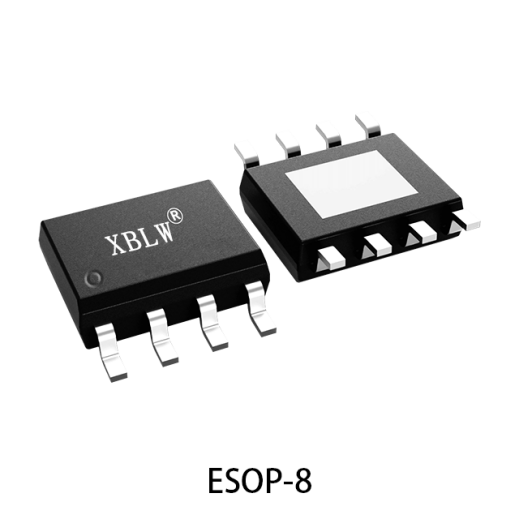
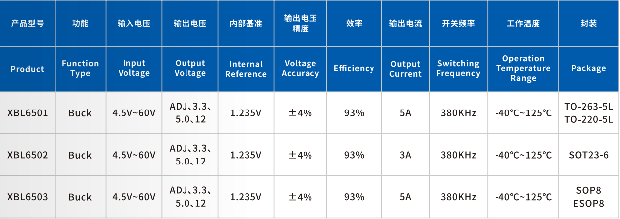
The XBL65 series chips includeXBL6501 ,XBL6502 andXBL6503 three products, respectively adoptingTO-220-5/TO263-5 ,SOT23-6 andSOP8/ESOP8 packages. These chips feature a wide input voltage range(4.5V~60V), large current output capability(max 5A), high efficiency(up to 93%), andmultiple protection functions, such asovercurrent protection andovertemperature protection. The following will introduce its application in POE networking equipment usingXBL6503-ADJ ESOP8 as an example.
02
Advantages of XBL6503 in POE devices
1. High-efficiency power conversion
XBL6503can achieve up to93%ofpower conversion efficiencyin POE devices.This means that when converting the input voltage to the voltage required by the device,energy lossis minimizedtomaximizetheutilization efficiency of electrical energy.
2. High current output capability
XBL6503has a maximum output current of5Aand can meet the relativelyhigh powerrequirements in POE devices.In some POE devices that require high power output, such ashigh-power wireless access pointsandnetwork cameras,XBL6503can provide sufficient current to ensure thestable operation of the device.
3. Small package size
XBL6503chip adoptsSOP8/ESOP8package, featuringa small sizecharacteristic. In POE devices, this small-sized package chip cansavecircuit boardspaceand make the device design morecompact。This is of great significance for some POE devices with strict requirements for volume and space.
4. Fast response and low ripple
The XBL65series canrespond quickly to load changes, ensuring that the system can stilloperatestably during voltage fluctuations.At the same time, this chip can providelow-rippleoutput, ensuring the output voltageremains stableand preventing system anomalies, andreducing electromagnetic interferenceto improve the system'sstability.
5. Multiple protection features
To ensure thesafe and stableoperation of the chip and system,XBL6503integrates multiple protection features, such as overcurrent protection,overtemperature protectionand others. These protection features can respond promptly to various abnormal conditions to prevent chip damage and system failure.
03
Actual application cases of XBL6503 in different application scenarios of POE devices
POE Separator
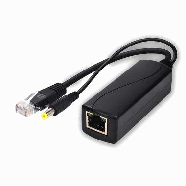
A POE splitter is used to separate power and data signals from Ethernet cables. It extracts48Vvoltage througha rectifier bridgeandfilter capacitorsand then uses a buck chipXBL6503toefficiently convertit into thelow voltagerequired by the device.XBL6503supportswide voltage inputandhigh output currentto ensurestable power supply。POE splitters are widely used in non-POE devices such as surveillance cameras, wireless access points, and IP phones, providinga stable power supplywhilemaintaining the integrity of the data signal.
Webcam

In POE network cameras,the XBL6503chip can provide stablehigh current output(up to 5A), meeting the high power requirements of the camera. Its efficient power conversion capability ensures the camera'sstabilityduringlong-term operation, while its small package size also makes the camera design morecompact.
Wireless Access Point
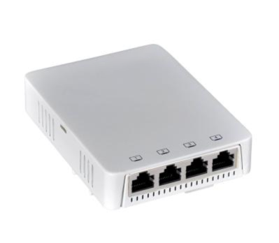
For high-power wireless access points,the XBL6503chip can provide sufficient current to ensure the device'sstable operationunder high load.Itsfast responseandlow ripplecharacteristics ensure the device operates normally during voltage fluctuations,improvingthe system'sreliability.
POE Switch
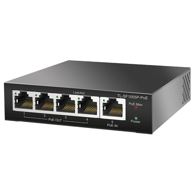
POE switchis a network device that cansimultaneouslytransmitpoweranddatavia Ethernet cables.It obtains powerfrom upstream devices (such as PSE)for its own operation, whileproviding powerto downstream devices (such as PD).The POE switch plays a key role in POE networks, ensuringthe effective transmissionof poweranddata signals, and is widely used indevices such assurveillance camerasand wireless access points.
Smart building automation equipment
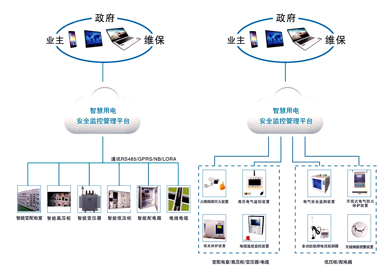
In smart building automation systems,the XBL6503chip can providestablepower support for varioussensors and controllers.Its multipleprotection functionsensure thereliability of the equipmentin harsh environments,extending theequipment's service life.
04
Scheme Design
How it works
This diagram is the physical connection schematic of a POE device. The working principle of a POE device is totransmit poweranddatasimultaneouslyoveran Ethernet cable.The fundamental reason it can achieve this is thatdifferential signaltransmission depends ondifferential voltage (V1 - V2), and adding a 48V voltage will not affect the normal transmission of the signal.
Its working components mainly include:PSE (Power Supply Unit) ,PD (Power Device) , DC-DC buck chips,rectifier circuit andresistors and capacitors , etc.
48V Power Supply Circuit
PSE (Power Supply Equipment) mainly provides48V powerconnected to the network transformer center tap. At this point, on top of the original signal voltage,addsthe48V DC voltage, becausethe signal transmission of network communication equipmentis determined by thedifferential voltageon the two lines. The differential voltage of the signal without the added 48V voltage can be calculated using the differential formula V1-V2. After the 48V voltage is added, substituting it into the formula (V1+48V)-(V2+48V)=V1-V2, it meansafter addingthe 48V voltagethe signal remains unchanged. Therefore, adding the 48V voltage will not affectthe normal transmission of the signal.
Filter rectifier circuit
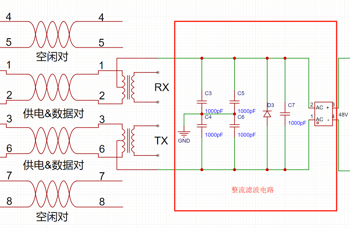
When the signal transmission entersthe PD (Power Delivery)after, the signal is connected todownstream devices via the network transformer, and the superimposed 48V voltage is taken from the center tap of the network transformer, at which point the voltage transmission is completed. Capacitors C3, C4, C5, and C6 are used tofilter and eliminate interference from the incoming 48V voltage. The main function of the rectifier bridge is topreventpolarity reversal caused byincorrect connectionorequipment failure andensure that the voltage input toXBL6503 has the correct polarity. In addition, the rectifier bridge cansmoothvoltage fluctuations andprevent damage to subsequent circuits from reverse current andvoltage spikes , improving the system'sstability andreliability . The rectifier bridge provides additional protection and stability
XBL6503-ADJ Buck Converter
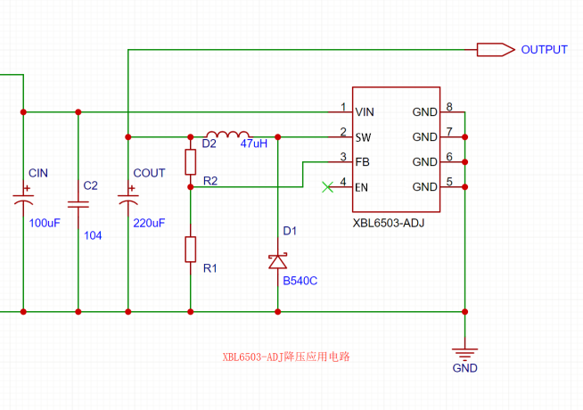
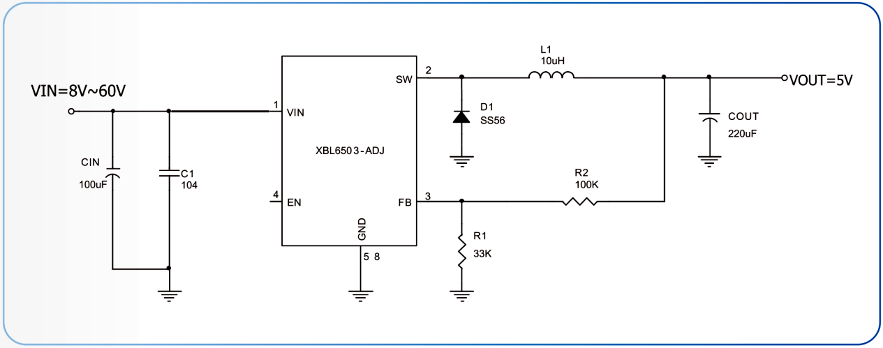
After the voltage passes throughthe rectifier circuitand is rectified,XBL6503-ADJis connected toefficiently and stablystep down the output to provide the appropriate voltage to power the downstream circuit. It should be noted that,the output voltage ofXBL6503is mainly determined byR2andR1throughvoltage division. The formula for selecting the resistors isVOUT=1.230(1+R2/R1) where R2=100KΩ.
XBL6503 Maximum Continuous Output Currentis5A, providingstrongloadcarrying capacityforsubsequentcircuits.Its4.5V~60V
XBL6503 Circuit Design Recommendations
VIN is the positive voltage input pin of XBL6503 . Here, it is necessary to add an appropriate capacitor to prevent peak voltage from damaging the chip. Here, it is recommended to use a 100uF electrolytic capacitor along with a 104
SW is an internal switch. The voltage on this pin switches between(+VIN - VSAT) and approximately- 0.5V, the duty cycle is approximatelyVout / Vin. To minimize coupling with sensitive circuits, the copper area connected to this pin should be minimized.
FB is a feedback pin. When used, it must be connected to a voltage divider resistor, which controls the output voltage according to the formulaVOUT=1.230(1+R2/R1), R2=100K .
ENThe foot is a switch pin. When the pin voltageis higher than 1.2Vorfloatingthenturns onthe output,and when it is lower than 0.6Vthenturns offthe output.
05
Selection Table
06
Summary
XBL6501/02/03series chips, with theirhighefficiencyandstablepower conversioncapabilities andmultiple protection features, provide an ideal power solution for POE devices. Their practical application cases in various scenarios demonstrate theirexcellent performance in meetinghigh power requirements,improvingsystem stabilityandreliability. With the widespread application of POE devices in various fields, theXBL6501/02/03series chips will surely become animportant driving force for the industry's development.
Recommend News

Follow Us


-
Phone
400-9682 003