
Xinbole Zero‑Drift, Bidirectional Current‑Sense Amplifier — XBLWINA199
Inpower management,battery charging,communication equipmentand other applications, accuratecurrent sensingisa core link to ensure stable system operation.Xinbole (XBLW)has launched a new product:high‑performancecurrent‑sense amplifier INA199, designed forhigh‑precision current monitoringscenarios.
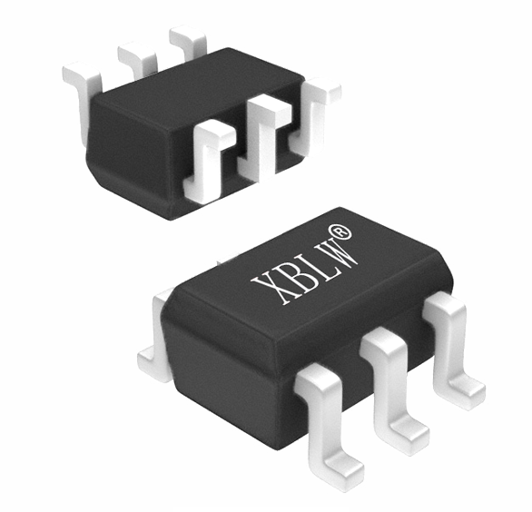
I. Product Overview
XBLWINA199 is ahigh‑precision current‑sense amplifierintroduced by Xinbole. It supports single‑supply2.7V to 30V power supplyand can detect the voltage drop across the sense resistor within the-0.2V to 30V common‑mode voltage range. This device is suitable for multiple fields includinghigh‑side and low‑side current sensing,battery charge management,power supply systems.
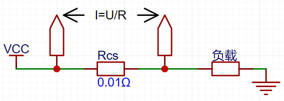
INA199 adoptszero‑drift architectureand featureslow offset voltageandhigh‑precision gaincharacteristics, meeting strict current‑monitoring requirements inindustrialandconsumer‑electronicsapplications.
II. Key Features
l Fixed gainoptions: 50V/V, 100V/V, 200V/V, corresponding to models INA199A1, A2, A3 respectively;
l Input offset voltage: max.±200μV;
l Input common‑mode voltage range:-0.2V to 30V;
l Supply voltage range:2.7V to 30V;
l Quiescent current: typical 110μA, suitable forlow‑power systems;
l Gain error: max.±1%over full temperature range;
l Temperature drift:offset voltage drift 0.5μV/°C, typical gain drift 3ppm/°C;
l Rail‑to‑rail outputfor wider output dynamic range;
l Package: SC70‑6, ideal for compact designs;
l ESD rating:±4kV (HBM)with good anti‑static performance;
l Operating temperature range: ‑40°C to +125°C, suitable for harsh environments.
III. Typical Application Scenarios
l Notebook power management
l Battery chargers
l Communication equipment
l Power management systems
l Qi‑standard wireless charging transmitters


IV. Pin Description
INA199 comes in a 6‑pin SC70 package. Main pins are listed below:
1. REF: Reference‑voltage input for setting output common‑mode voltage;
2. GND: Power ground;
3. V+: Positive power‑supply pin; connect a 0.1μF bypass capacitor;
4. IN+: Positive input of sense resistor;
5. IN‑: Negative input of sense resistor;
6. OUT: Voltage output.
V. Operating Principle and Configuration
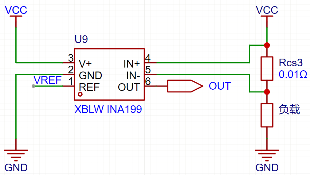
The core of INA199 is adifferential‑amplifier structure, and its output follows the formula:
OUT = R1/R3(Iload * Rshunt)+REF
By configuring the voltage on the REF pin, you can implementunidirectionalorbidirectional current sensing:
1. REF tied to GND: output rises linearly withpositive current;
2. REF tied to V+: output falls linearly withnegative current;
3. REF tied to (V+)/2: supportsbidirectional positive‑negative current sensing.
In bidirectional‑sensing applications, if REF is supplied by resistor voltage‑divider, it is recommended to add avoltage buffertoimprove accuracy.
VI. Performance Highlights
Thezero‑drift architectureof INA199 enablesultra‑low offset‑voltage driftundertemperature variation, which is especially suitable forsystems requiring long‑term stability. Its gain error is only±1%over full temperature range. Combined with3ppm/°C typical gain drift, it guaranteessensing consistency across wide temperature range.
In addition, bandwidth is gain‑dependent: INA199A1 (50V/V) features 50kHz bandwidth, while A3 (200V/V) offers 20kHz. Users can select flexibly according to response‑speed and amplification‑factor requirements.
VII. Summary
XBLWINA199 is acurrent‑sense amplifierintegratinghigh precision,low power consumption,wide voltage range. It fits diversehigh‑side / low‑side current‑monitoring scenarios. Itszero‑drift feature and fixed‑gain optionssimplify system designandimprove measurement reliability.
Whether for portable devices, communication base stations or wireless‑charging systems, INA199 delivers stable and accurate solutions for current‑sensing tasks.
Recommend News


Follow Us


-
Phone
400-9682 003