
ChipBioDC-DC Chip MC34063: A Guide to Multi-Topology Circuit Design and Engineering Implementation
In the field of low-to-medium power switching power supply design, the MC34063 is a classic device familiar to hardware engineers. This integrated DC-DC control chip is widely used in scenarios such as auxiliary power supply for industrial instruments , dual power supply for analog circuits , charging of small energy storage devices , and multi -channel low-voltage power supply , thanks to its advantages such as simplified peripheral circuits, strong functional adaptability , and integrated protection circuits .
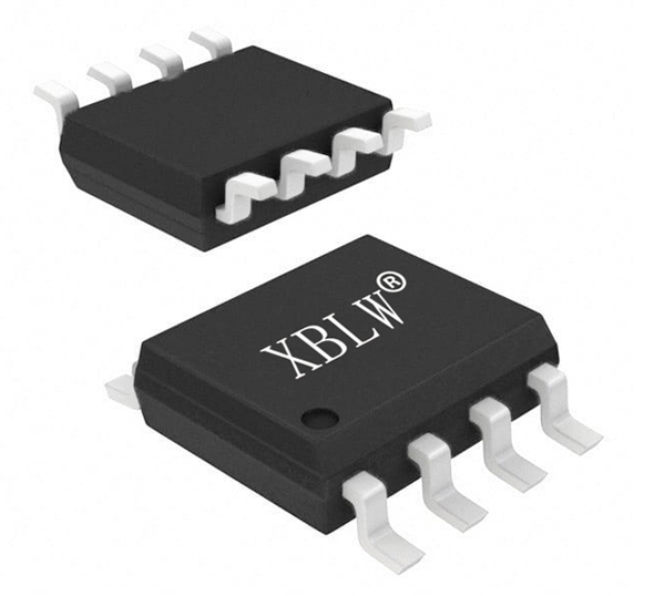
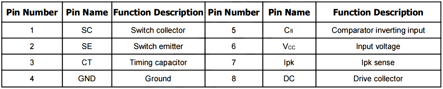
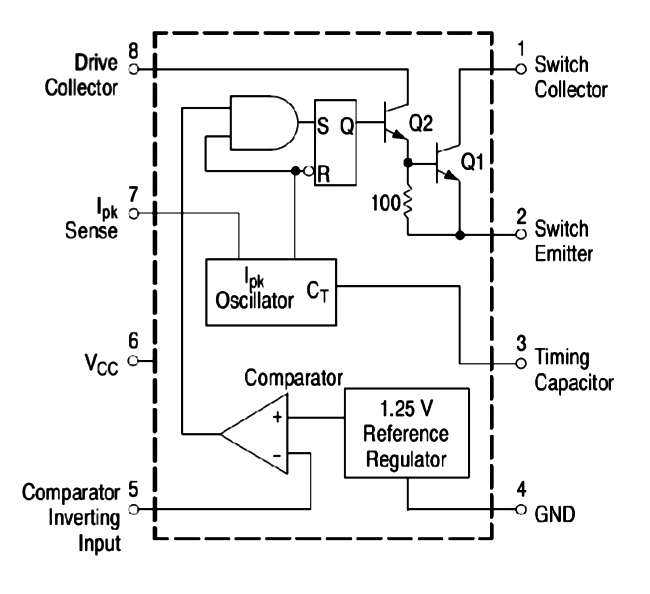
The MC34063 is a bipolar integrated controller that integrates a temperature-compensated reference source , a controllable oscillator , a comparator , and a 1.5A high-current switch . It supports a wide input range of 3~40V , and its operating frequency can be flexibly adjusted from 100Hz to 100kHz. It features built-in short-circuit current limiting protection and is suitable for most common low-power power supply requirements . Pin 3 is the timing capacitor terminal, determining the circuit's switching frequency; pin 5 is the feedback input terminal, which, in conjunction with the voltage divider resistor, stabilizes the output voltage; pin 7 is the current sensing terminal, achieving precise current limiting based on a 300mV threshold, and is the core pin for circuit protection.
The chip can be used to build:buck,boost, andpolarity inversion circuits. These are the three standardDC-DC topologies, also the three most commonly used schematics in engineering. The three circuitshave similar basic architectures, differing only in the connection methods of the energy storage inductor and freewheeling diode. The output voltage can beprecisely configured using voltage divider resistors. The general calculation formula is:
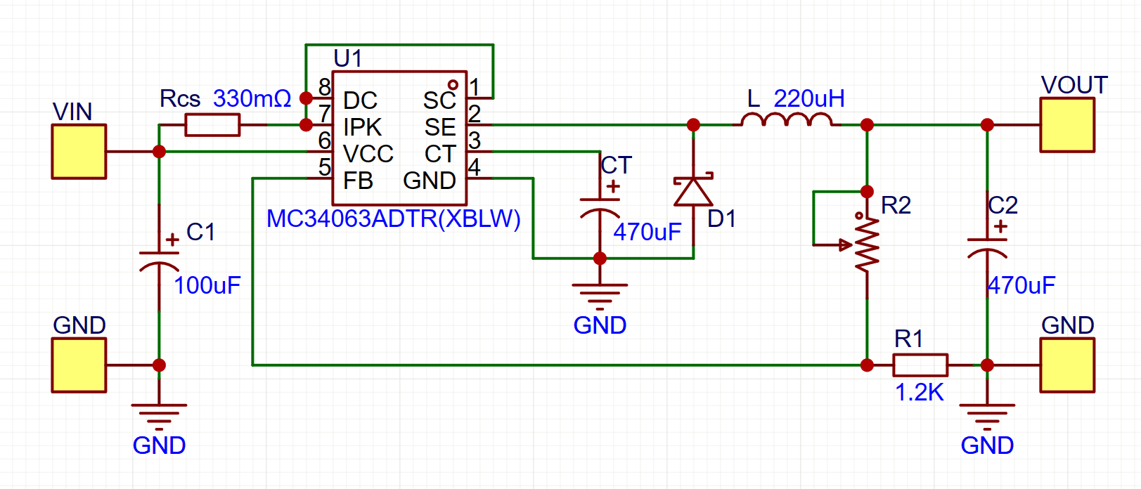
Vout = 1.25 * (1 + R2 / R1)。
Buck converters are the preferred choice for low-voltage output applications such as MC34063 as its core, supplemented by24V to 5V and 12V to 3.3Va voltage divider resistor network,a Schottky freewheeling diode,input and output filter capacitors , an energy storage inductorand. The input voltage is connected to pin. The schematic uses the6 of the chip, a sampling resistor is connected in series at pin 7 for current limiting, and the output voltage is sampled at pin 5 to ensure stable output.
Boost circuits are suitable for low-voltage to high-voltage applications . By adjusting the wiring order of the inductor and diode , the output voltage can reach up to twice the input voltage , making it the mainstream solution for low-power boost power supply .
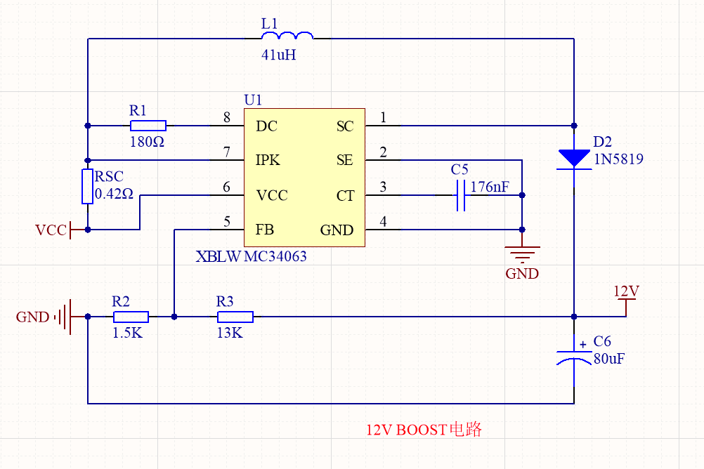
The polarity reversal circuit is used to generate negative voltage to meet the dual power supply requirements of operational amplifiers and analog chips . The circuit adopts a Cuk topology, which has good input and output current continuity and excellent electromagnetic interference performance .
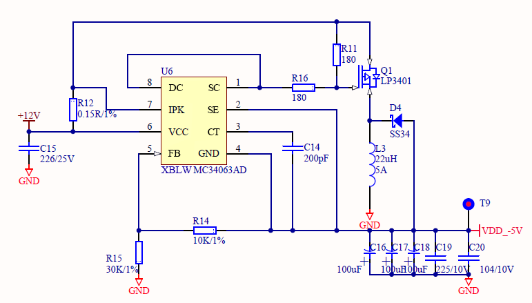
For high-current load requirements , an external transistor or power MOSFET can be connected to the basic circuit to build a current-amplifying circuit . Using Darlington or anti-saturation drive methods can both expand the output current and ensure switching response speed, adapting to higher power supply scenarios .
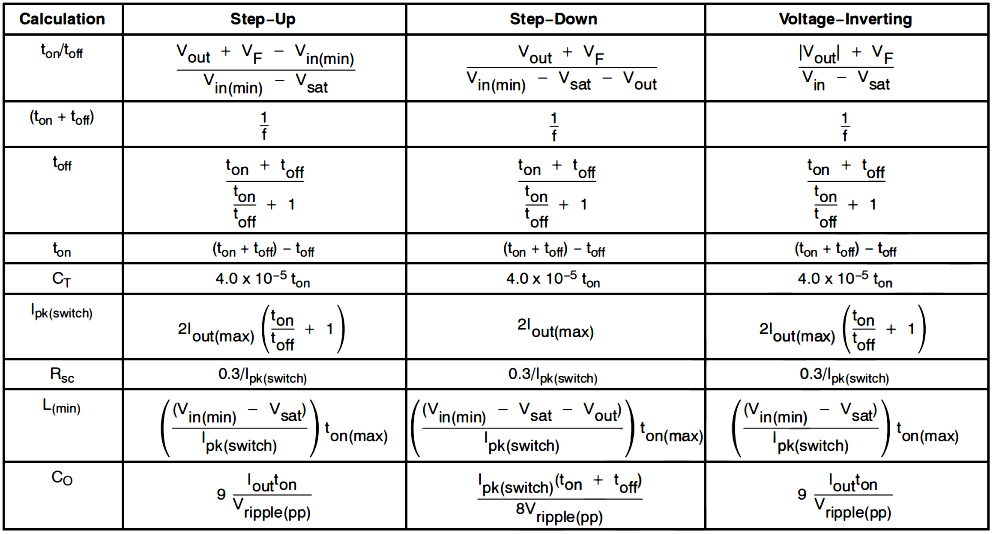
Circuit parameter calculation is the core of the design. Commonly used engineering formulas can quickly determine the parameters of peripheral components: the timingcapacitorCTdeterminesthe switching frequency; the current limiting resistor is calculated according toRsc = 0.3V / Ipk; in terms of component selection, Schottky diodes are preferred for freewheelingdiodes,multi-strand parallel-wound inductors are selected to weaken the skin effect in high-frequency operation, and high-frequency capacitors are matched at the outputto reduce ripple.
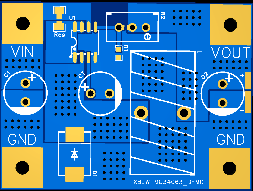
PCB layout should followthe principle of minimizing high-frequency loops:the traces of high-current loopscomposedofswitching transistors,inductors , and diodes should be shortened as much as possible , andthe trace length of the SW switch node should be controlled within 5mm; the feedback resistor should be placed close to pin 5, and the sampling point should be taken from both ends of the output capacitor to ensure sampling accuracy;andheat dissipationspace should be reserved to furtherimprove circuit stability.the copper foil in the power area should be appropriately widened
From basic voltage conversion to customized functional circuits,the MC34063, with itsflexible topology expansion capabilitiesandsimple hardware design, has become the preferred choice for low-cost, low-to-medium power supply designs. A thorough understanding of itscircuit architecture,parameter calculations , andlayout specificationsallows for efficient implementation in various conventional power supply projects, and it also serves as an excellent practical tool for beginners learning about switching power supplies.
Recommend News


Follow Us


-
Phone
400-9682 003