
BUCK BOOST Topology Analysis: Principles, Component Selection, and Design
In DC/DC converter circuits, the BUCK BOOST topology, with its ability to step up and down and its simple circuit structure , has become a core choice for industrial power supplies , automotive power supplies , and negative voltage output scenarios . It can achieve an output voltage lower or higher than the input, its only characteristic being that the output voltage polarity is opposite to the input. This article completely breaks down the entire BUCK BOOST topology design process , covering its working principle and engineering considerations .
I.BUCK BOOST Topology Core Structure and Working Logic
The BUCK BOOST standard topology consists a power transistorQ1,a freewheeling diodeD1,an energy storage inductor,an output capacitor, anda loadR1. It isa non-isolated topologythat achieves step- ofup and step-down voltage based on inductorenergy storage/release.
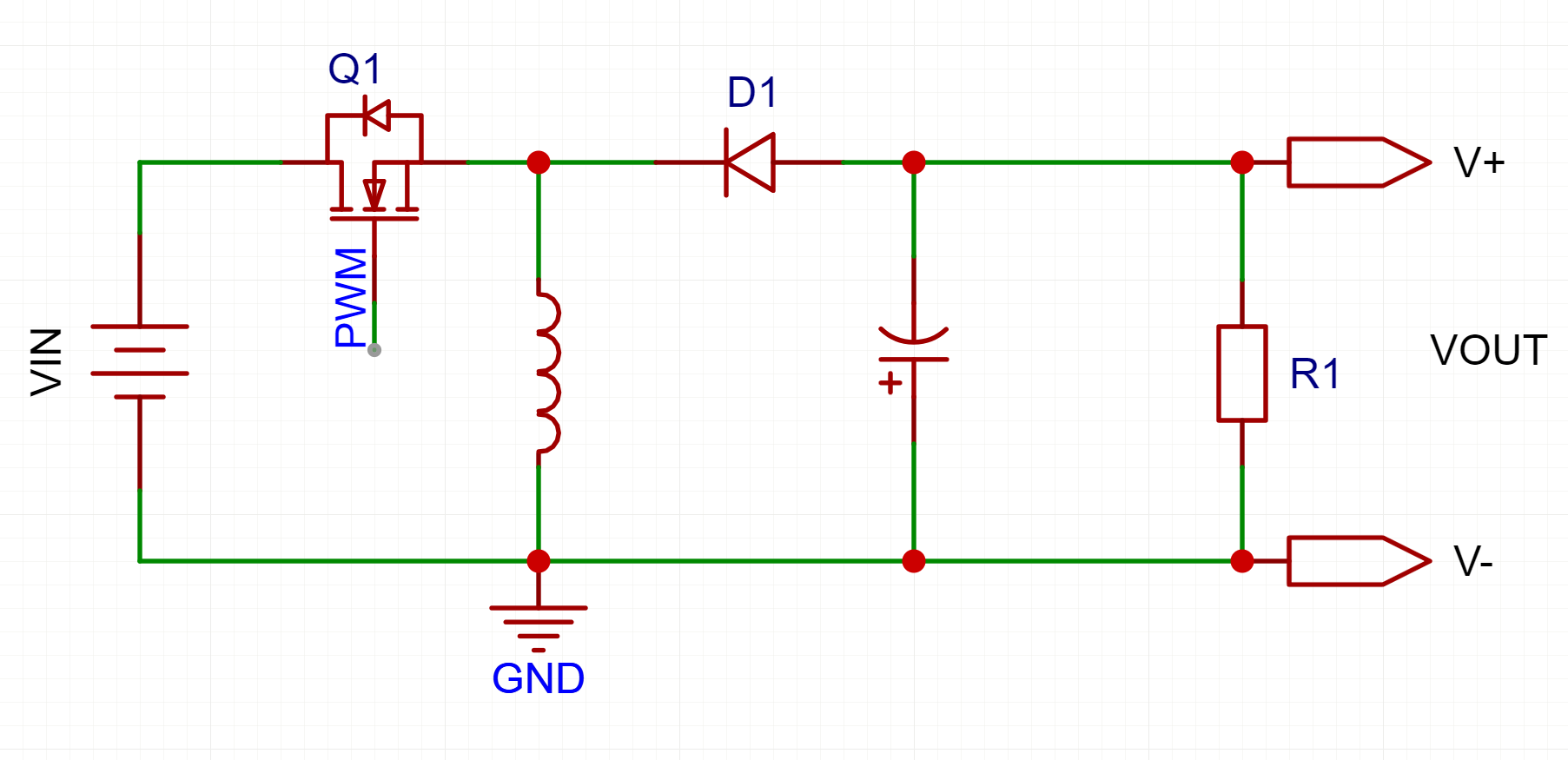
The circuit operates in two steady-state phases, adhering tothe inductance volt-second conservation rule throughout :
1. Power transistor Q1 conduction stage
InductorL1is directly connected tothe input power supply, and the voltage across its terminalsis VIN. The inductor current rises linearly,completing energy storage.
The freewheeling diodeD1 is reverse biasedand cut off , providing electrical isolationbetween the output and input sides .
The output capacitor COUT discharges and continues to supply power to the load R1 , ensuring that the load is not interrupted or disconnected.
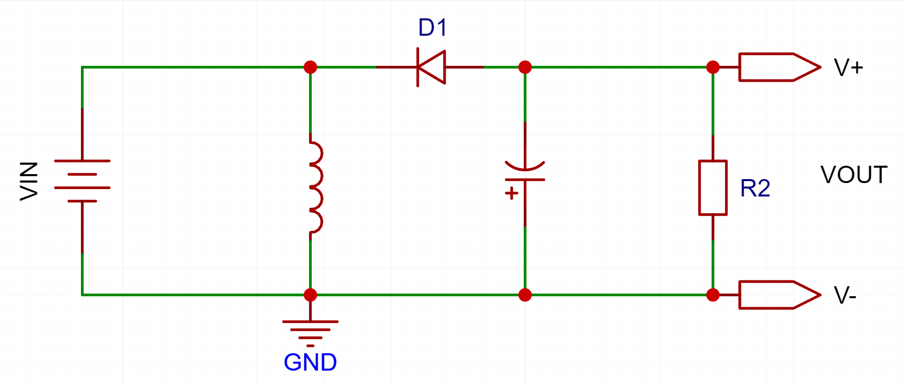
2. Power transistor Q1 turn-off stage
The inductor current cannot change abruptly, so it releases energy to the output side through D1 .
The inductorchargesthe output capacitorCOUTand simultaneouslysupplies power to the load, thus completingthe energy transfer.
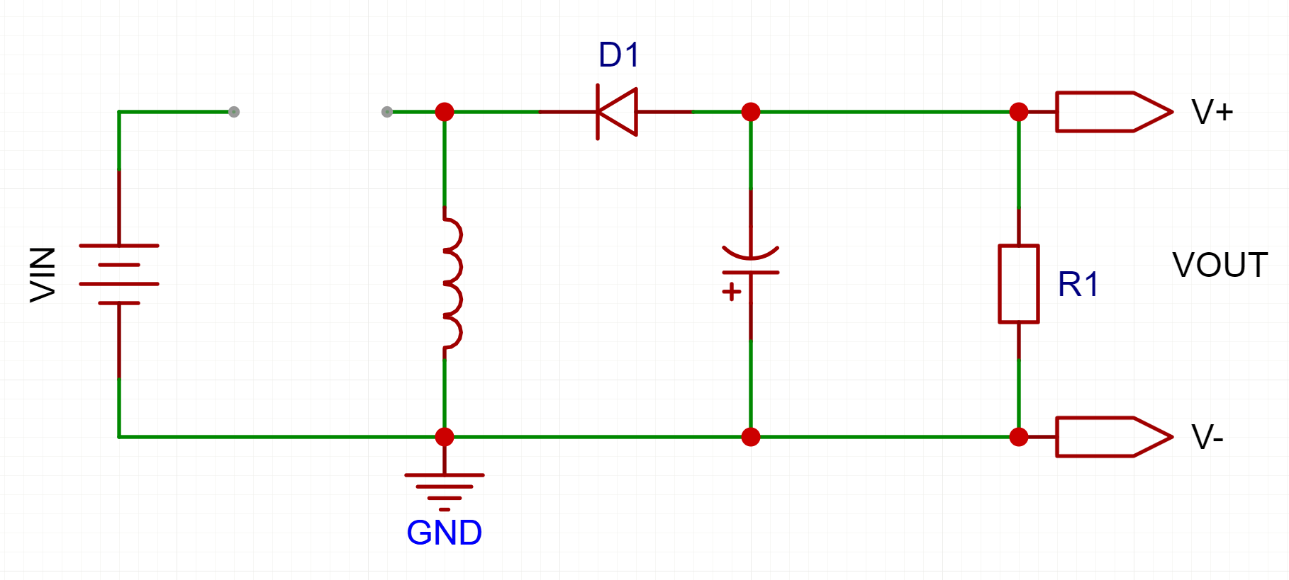
Duty cycle and buck/boost voltage correspondence
D < 0.5: Output voltage absolute value < input,buck mode.
D > 0.5: Output voltage absolute value > input,boost mode.
II. Calculation and Selection of Key Components
Device parameters directly determinecircuit stability,efficiency, andreliability. The following are engineering calculation methods:
L1 energy storage inductor
Sensitivity calculation formula:L = (D×VIN)/(0.3×FSW×(IIN+IOUT))
Peak inductor current:ILPEAK = 1.15 × (IIN + IOUT)
Selection requirements:Rated current≥ 1.5 × (IIN + IOUT), with sufficient safety margin.
2. Freewheeling diode D1
Reverse withstand voltage:VD = VIN + |VOUT|, with a 1.5 times withstand voltage margin when selecting a model.
Current capability: Average current= IOUT, Peak current = ILPEAK
Recommendation:Schottky diodes, to reduce conduction losses and improve efficiency.
3. Power transistor Q1 (MOSFET)
Withstand voltage:VMOS = VIN + |VOUT|
Current capability: Peak current= ILPEAK, Average current = IIN
Prioritize devices with low Rds(on) to reduce conduction losses.
4. Input/Output Capacitors
The capacitance value is calculated based on voltage drop requirements, prioritizing lowESR capacitors to suppress ripple.
III. Important Notes for Engineering Applications
1. Core Principle of Pressure Resistance
The withstand voltage of power transistors and freewheeling diodes must be greater thanthe absolute value of the sum of the input voltage and the output voltage;full-capacity operation is strictly prohibited.
2. Grounding Design
The chipsignalGNDandpower ground are strictly separatedto avoidground bounce noiseinterfering with the chip's operation.
3. Input Filtering
The chip's power supply is equipped witha filter capacitor of 10μF or higher to ensurea clean power supply.
4. Efficiency and Margin
BUCK BOOST is less efficient than pure BUCK/BOOST, andsufficient marginsmust be made , andheat dissipation.in device current,power
5. Load power supply continuity
The output capacitor provides freewheeling current during the conduction phase, andits capacitanceandESRdirectly affectthe output rippleandload stability.
IV. Summary
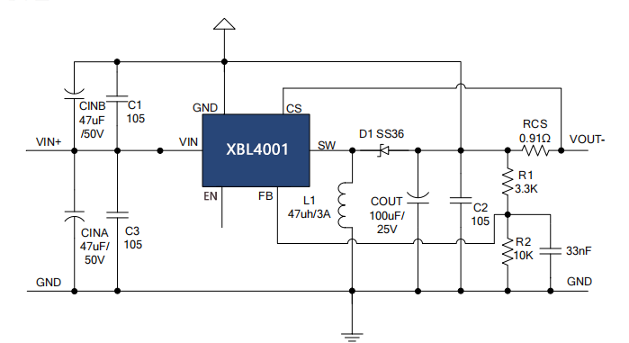
The BUCK BOOST topology is simple and flexible , making it an ideal solution for negative voltage output and wide-range step-up/step-down conversion . The core design considerations lie in the application of the volt-second balance formula, control of component margins , and grounding and filtering design .
Recommend News

Follow Us


-
Phone
400-9682 003