
XBLW XOPA333 / XOPA2333 Zero‑Drift CMOS Op‑Amplifier Technical Article
In precision‑signal acquisition, sensor‑interface and battery‑powered systems, operational‑amplifier requirements keep rising: ultra‑low offset voltage & drift, plus a good balance of low power consumption, wide supply‑voltage range and high noise immunity. XBLW’s XOPA333 (single‑channel) and XOPA2333 (dual‑channel) zero‑drift CMOS op‑amps feature 15 µV ultra‑low offset voltage, 350 kHz bandwidth and 26 µA ultra‑low quiescent‑current, making them ideal candidates for industrial‑control, medical‑equipment and precision‑measurement applications.
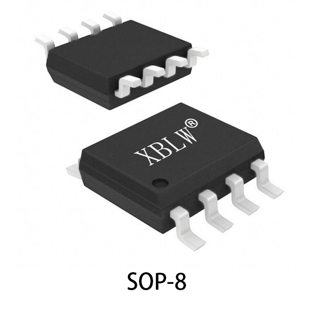
1. New‑Product Introduction: XOPA333 / XOPA2333 Series
XOPA333/XOPA2333 are XBLW high‑performance zero‑drift op‑amps built with advanced chopper‑stabilization technology. They measure and compensate input‑offset‑voltage in real‑time, eliminating drift induced by time‑and‑temperature variation as well as 1/f‑noise effects. Typical offset‑voltage drift is only ±50 nV/℃, ensuring high accuracy across full operating‑temperature range.
2. Key Specifications
- Superior DC precision: Input offset voltage down to max ±15 µV
- Ultra‑low drift: Max ±50 nV/℃
- High open‑loop gain: 112 dB
- Low power: 26 µA quiescent‑current per channel
- Wide supply‑voltage range: 1.8 V to 5.5 V
- Rail‑to‑rail I/O: Supports high‑side and low‑side signal sensing
- Enhanced EMI protection: Improves system noise immunity
- ESD protection: 5 kV HBM, suitable for industrial‑grade applications
3. Application Scenarios
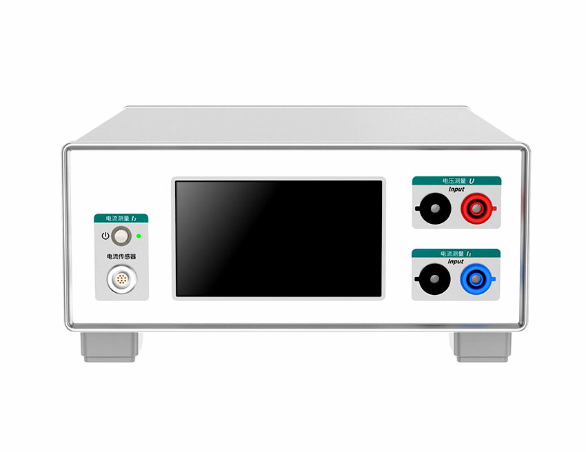
- Precision current‑sensing
- Temperature, pressure and position sensors
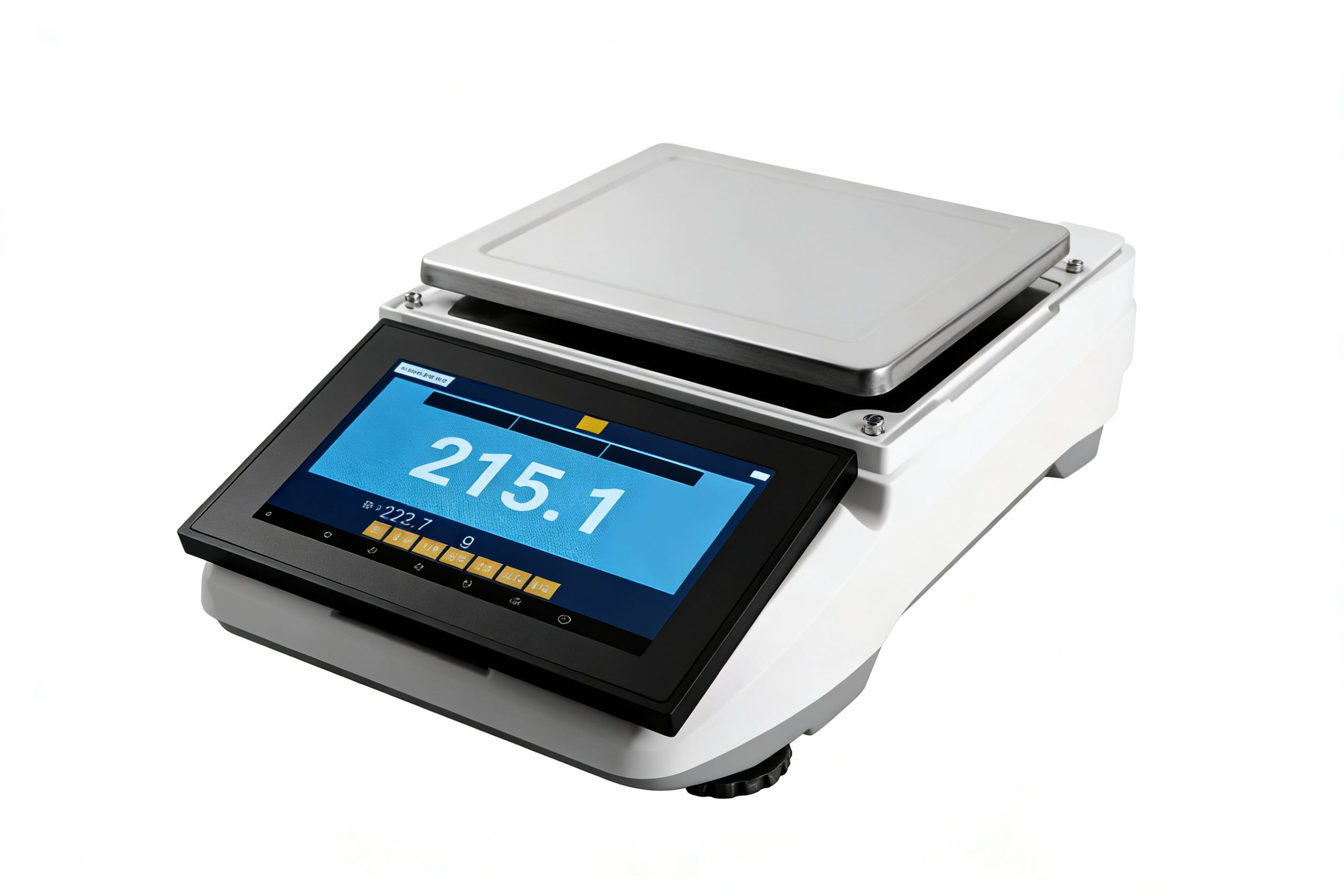
- Medical instruments (e‑scales, clinical thermometers etc.)
- Thermocouple amplifiers
- Strain‑gauge signal‑conditioning
4. Circuit‑Design Guidelines
▪ Low‑Side Current‑Sensing Circuit
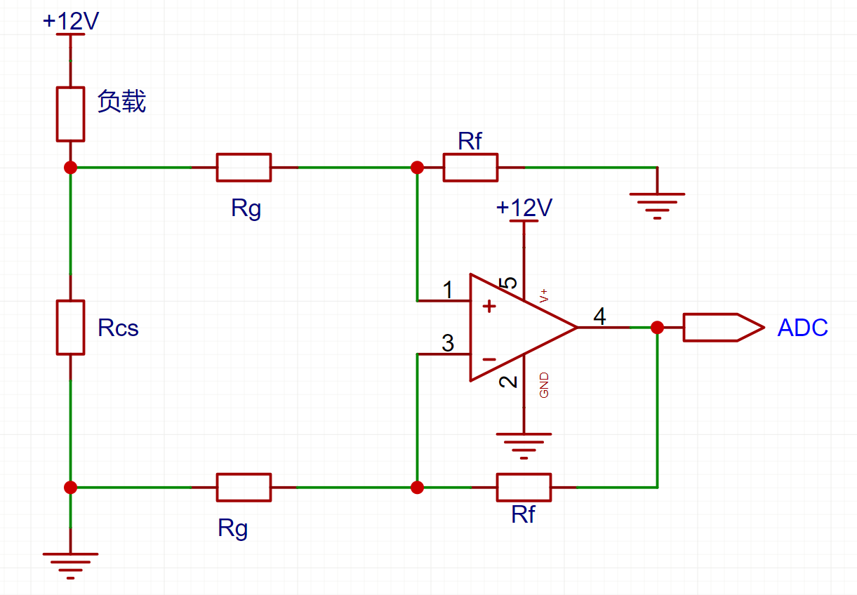
XOPA333 is well‑suited for low‑side current‑sensing. The above schematic shows a typical implementation. Gain is set by R2/R1, formula: Vout = (1 + Rf/Rg) × (I_load × Rcs). Output is proportional to load‑current, ideal for battery‑management systems and power‑supply monitoring.
▪ Differential‑Amplifier Circuit
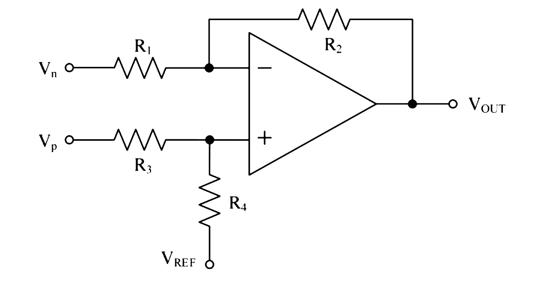
This is a differential‑signal amplifier circuit. With matched resistors R1=R3, R2=R4, output follows: Vout = R2/R1 × (Vp‑Vn) + VREF. Thanks to XOPA333/XOPA2333 zero‑drift (auto‑calibration), ultra‑low offset‑voltage / drift and high CMRR, this circuit achieves accurate small‑differential‑signal amplification with minimal error.
5. Device‑Selection Guide
Part Number | Channels | Package | Bandwidth | Iq | Offset Voltage | Typical Use‑Case |
XOPA333AIDBVR | Single | SOT23‑5 | 350 kHz | 26 µA | ±15 µV | Precision sensors, portable equipment |
XOPA333AIDR | Single | SOP‑8 | 350 kHz | 26 µA | ±15 µV | General‑purpose precision amplification |
XOPA2333AIDR | Dual | SOP‑8 | 350 kHz | 26 µA | ±15 µV | Differential‑amp, current‑sensing |
XOPA2333AIDGKR | Dual | MSOP‑8 | 350 kHz | 26 µA | ±15 µV | Space‑constrained high‑precision designs |
6. PCB Layout Recommendations
To realise full performance from XOPA333/XOPA2333, follow these PCB‑layout best‑practices:
1. Mitigate thermocouple effects: Use homogeneous conductor materials on input paths and maintain uniform temperatures to suppress Seebeck‑voltage‑induced offset.
2. Guard‑ring implementation: Place guard ring around input pins, connect to non‑inverting input to reduce leakage current.
3. Isolate input / output: Avoid parallel input‑output traces to minimise parasitic‑capacitance positive feedback.
4. Ground‑plane design: Solid ground plane improves thermal dissipation & noise immunity; avoid ground‑loop formation within sensitive input sections.
5. Power‑supply decoupling: Place 0.1 µF ceramic capacitor close to each power‑supply pin to suppress power‑rail noise.
7. Cross‑Reference vs. Overseas Competing Devices
Part Number | Vendor | Offset Voltage | Bandwidth | Iq | Remarks |
XOPA333 | XBLW | 3 µV | 350 kHz | 26 µA | Zero‑drift, rail‑to‑rail, low‑power |
AD8628 | ADI | 1 µV | 2.5 MHz | 850 µA | Higher bandwidth, higher supply‑current |
AD8551 | ADI | 1 µV | 1.5 MHz | 850 µA | High precision, for instrumentation |
OPA333 | TI | 2 µV | 350 kHz | 17 µA | Comparable performance, higher cost |
MCP6V01 | Microchip | 2 µV | 1.3 MHz | 300 µA | Higher bandwidth, higher current draw |
AS333 | Diodes | 8 µV | 350 kHz | 17 µA | Comparable performance, higher cost |
NCS333 | ONSEMI | 3.5 µV | 350 kHz | 21 µA | Comparable performance, higher cost |
Delivering high precision together with compelling cost‑performance, XBLW XOPA333/XOPA2333 represent an excellent domestic alternative to imported op‑amp brands.
8. Summary
XBLW XOPA333/XOPA2333 zero‑drift op‑amps feature ultra‑low offset‑voltage, ultra‑low drift, low power‑consumption and wide supply‑voltage range. They are widely deployed within precision‑measurement and industrial‑control applications. Whether used for current‑sensing, sensor‑amplification or general‑purpose signal‑conditioning, XOPA333/XOPA2333 deliver stable and reliable system‑level performance, enabling engineers to strike an optimum balance between cost and performance.
Recommend News


Follow Us


-
Phone
400-9682 003