
I. Product Overview
In microcontroller systems, I/O resources are often limited. The SN74HC595, a 8-bit serial-in, serial-out, shift register, offers built-in registers and tri-state outputs, enabling the expansion of 8 parallel outputs using only 3 I/O ports. This significantly improves port utilization and is ideal for applications such as multi-LED displays, key scanning, and industrial control.
II. Key Features
- 8-bit serial input, capable of being cascaded to extend the number of outputs.
- Independent clock control: Separate control of the Shift Clock (SHCP) and the Storage Clock (STCP).
- Three-state output: Enables and disables output, facilitating use in bus applications.
- Asynchronous reset: The master reset pin can clear the shift register.
- Wide operating voltage: 2.0V-6.0V, compatible with 3.3V/5V systems
- Wide temperature range: -40°C to +125°C, suitable for various working environments
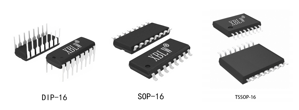
- Available in DIP-16, SOP-16, and TSSOP-16 packages.
3. Pin Function Description
Part number | Symbols | Features and Functionality |
1 | Q1 | Parallel data output 1 |
2 | Q2 | Parallel data output 2 |
3 | Q3 | Parallel data output 3 |
4 | Q4 | Parallel data output 4 |
5 | Q5 | Parallel data output 5 |
6 | Q6 | Parallel data output 6 |
7 | Q7 | Parallel data output 7 |
8 | GND | Ground |
9 | Q7S | Serial data output (for cascading) |
10 | MR | Main Reset (Low-Level Active) |
11 | SHCP | Shift register clock (rising edge active) |
12 | STCP | Storing the clock signal (rising edge only, latching) |
13 | OE | Output Enable (Low-level active, high-level output) |
14 | DS | Serial data input |
15 | Q0 | Parallel data output: 0 |
16 | VCC | Positive power supply (2V~6V) |
IV. Detailed Explanation of Operation
The SN74HC595 contains two independent registers:
1. Shift Register: Responsible for receiving and shifting serial data.
2. Storage Registers: Store and control data for parallel output.
5. Workflow:
- The data is transferred from the DS pin to the shift register on the rising edge of the data signal.
- On the rising edge of the STCP signal, the data in the shift register is transferred to the storage register.
- When the OE (Output Enable) signal is low, the data stored in the registers appears on the parallel output lines Q0-Q7.
- The low voltage can asynchronously clear the shift register.
6. Truth Table for Function
Control | Input | Output | Features and Functionality | ||||
SHCP | STCP | OE | MR | DS | Q7S | Qn | |
X | X | L | L | X | L | NC | For low-capacitance applications, the effect is primarily on the shift register. |
X | ↑ | L | L | X | L | L | Clear the shift register and transfer its contents to the output register. |
X | X | H | L | X | L | Z | Clear the shift register, and output to a high-impedance state. |
↑ | X | L | H | H | Q6S | NC |
|
X | ↑ | L | H | X | NC | QnS | The content of the shift register is transferred to the hold register and then output through the output port. |
↑ | ↑ | L | H | X | Q6S | QnS | The contents of the shift register are shifted into the destination register, and the previous contents of the shift register are now stored in the destination register and output. |
| |||||||
VII. Key Electrical Parameters
Limit parameters
- Power supply voltage: -0.5V to +7.0V
- Input/Output Voltage: -0.5V to VCC + 0.5V
- Operating temperature: -40°C to +125°C
- Storage temperature: -65°C to +150°C
Recommended working conditions
- Power supply voltage: 2.0V to 6.0V
- Input voltage: 0V to VCC
- Output voltage: 0V to VCC
When more output is needed, multiple SN74HC595 chips can be cascaded together.
- The Q7S in the first section is connected to the DS in the second section.
- All SHCP, STCP, MR, and OE chips are connected in parallel.
- The microcontroller's three I/O pins can control an unlimited number of cascaded chips.
VIII. Important Considerations for Use
1. Decoupling capacitor: Place a 0.1μF ceramic capacitor between VCC and GND, close to the chip pins.
2. Unused input pins should not be left floating; they should be connected to VCC or GND.
3. Reset Function: Upon power-up, a brief, low-pulse signal can be applied to the MR to ensure a defined initial state.
4. Clock Edge: Data enters the SHCP clock edge on the rising edge, and is stored on the STCP rising edge. Pay attention to timing synchronization.
5. Output Enable: OE low is active, and can be permanently grounded to enable the output.
6. Cascading Attention: When cascading, the data transmission order is: first send the data from the last chip.
9. Typical Application Scenarios
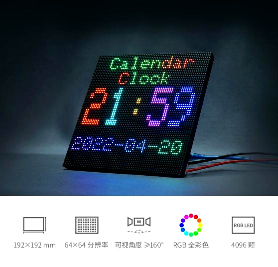
- LED matrix display: Multiple segments, each driven by a 16x16 matrix.
- Digital display with dynamic scanning: Utilizing MOSFETs for multi-digit display.
- Industrial I/O expansion: Extending the digital output capabilities of PLCs and industrial control panels.
- Relay control: Using a Darlington transistor to drive multiple relays.
- Serial communication interface conversion: Converting serial data into parallel control signals
Ten. Summary
The XBLW SN74HC595 is a classic shift-and-add chip, favored by engineers for its simple control, flexible expandability, and stable performance. It's a valuable solution for managing limited I/O resources, whether for basic LED control or complex industrial control systems.
Recommend News

Follow Us


-
Phone
400-9682 003