
High‑Efficiency 3A Step‑Down Solution: XBL2596 PCB Design Guide
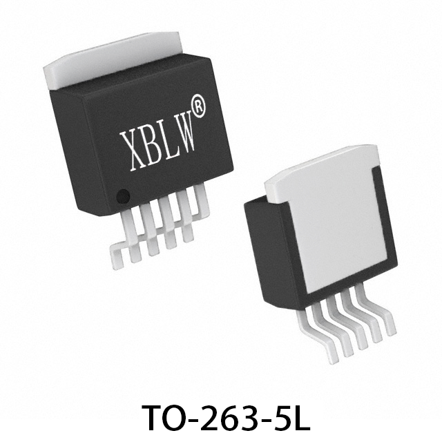
Within power‑supply design, high efficiency, large output‑current capability and excellent load‑regulation performance represent core design metrics. For 3A output‑current applications, the XBL2596 step‑down converter delivers a stable and reliable power‑conversion solution. Furthermore, properly‑optimized PCB layout is critical for XBL2596 to achieve its full datasheet‑specified performance.
1. Overview of Key Chip Features
XBL2596 is a 150 kHz fixed‑frequency PWM Buck DC/DC converter with the following characteristics:
- Wide input‑voltage: DC 4.5V ~ 40V
- Output options: Fixed 3.3V, 5V, 12V and adjustable (ADJ) output
- Maximum output current: 3A
- Typical conversion efficiency: up to 90%
- Operating frequency: Fixed 150 kHz; automatically drops to 50 kHz under secondary current‑limit condition
- Built‑in functions: PWM control, enable control, over‑current protection, internal frequency compensation
- Package types: TO‑263‑5, TO‑220‑5
2. Typical Application‑Circuit Design
XBL2596 supports two output modes with simple circuits and few external components:
1. Fixed‑output mode (3.3V / 5V / 12V)
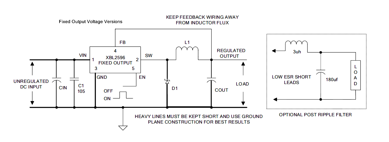
Well‑suited for applications requiring tight output‑voltage accuracy.
2. Adjustable‑output mode (ADJ)
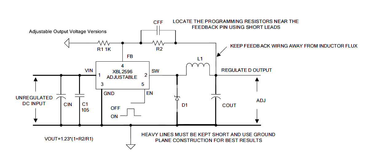
Output voltage is configured via external divider resistors R1, R2 for non‑standard‑voltage requirements.
> Design Note: Keep EN pin low or floating to maintain active output state.
3. Key Peripheral‑Component Selection
3.1 Feedback Resistor R1
1kΩ, 1%‑tolerance resistor is recommended for stable output voltage and good line‑regulation performance.
3.2 Input Capacitor C1
Place close to VIN and GND pins to suppress input‑side voltage noise and switching ripple.
3.3 Compensation Capacitor CFF (for ADJ or high‑output‑voltage conditions)
- Usage conditions: Output voltage >10V, or low‑ESR output capacitor (solid / tantalum capacitor)
- Capacitance range: 100pF ~ 33nF
- Formula: CFF = 1 / ( 31 × 1000 × R2 )
- Material recommendation: X7R / C0G ceramic, film or mica capacitors. Avoid Z5U‑type ceramic capacitors (poor temperature‑voltage stability).
4. PCB Layout & Thermal‑Management Recommendations
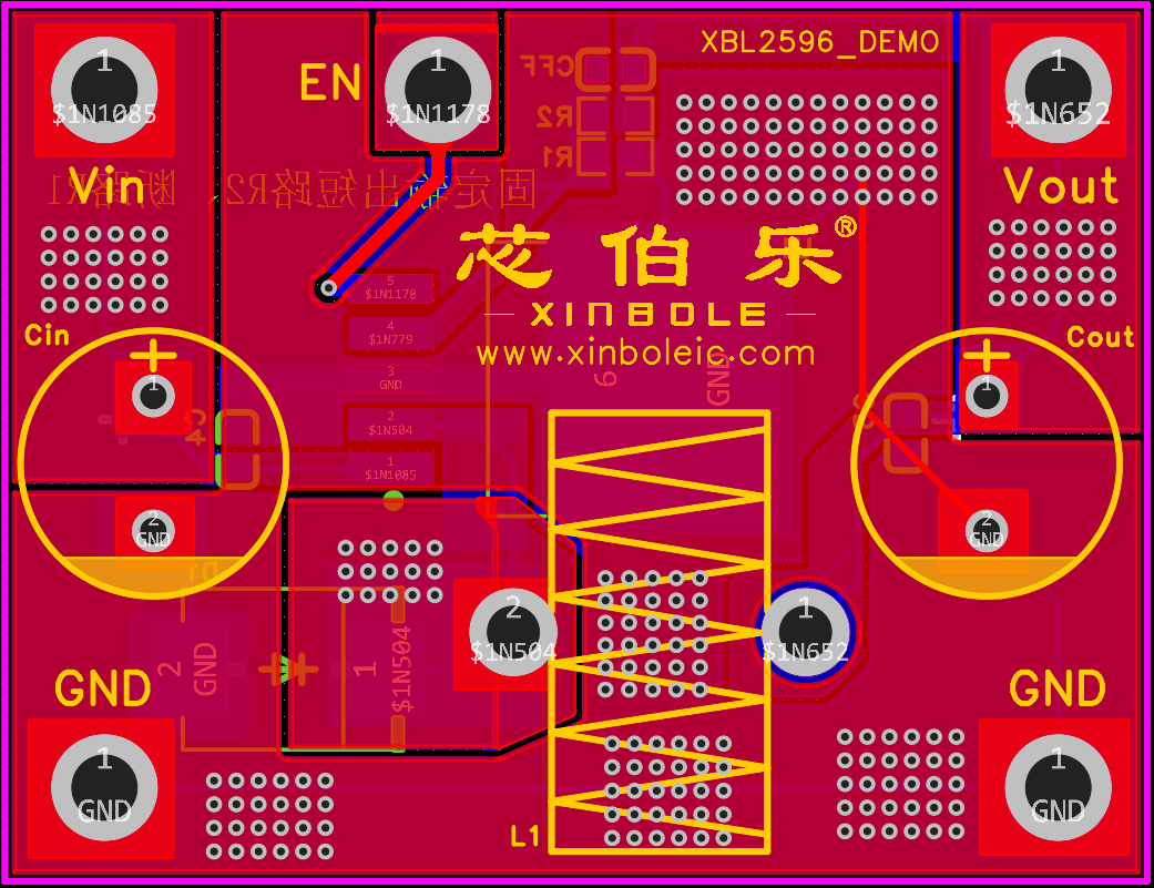
Sound layout practice is essential for stable operation:
- Feedback‑network routing: FB pin and feedback resistors shall be placed close together. Use short, direct traces routed away from switching nodes and high‑frequency noise sources.
- CFF placement: Place right beside feedback resistor R2 to minimize parasitic‑inductance effects.
- Thermal handling:
Under heavy‑load conditions, pour large ground copper underneath IC body and add thermal vias.
Single‑sided PCB is preferred for better electrical isolation and uniform thermal distribution.

5. Component‑Selection Reference Tables
Schottky‑Diode Selection Table

Capacitor‑Value Table (Adjustable‑Output Version)

Capacitor‑Value Table (Fixed‑Output Version)

The tables above list recommended Schottky diodes and input / output capacitor values for fixed‑ and adjustable‑output variants. Select components according to actual input‑output voltage, load‑current and ambient‑temperature conditions.
6. Application Scenarios
XBL2596 is well‑suited for:
- Automotive‑electronic equipment
- Industrial‑control & sensor power supplies
- Battery‑powered portable devices
- Distributed power‑supply systems
- Module power supplies requiring high input‑voltage and compact‑size constraints


Conclusion
Delivering up to 3A output current with up‑to‑90% efficiency and good load‑regulation performance, XBL2596 provides engineers with a reliable step‑down power‑conversion solution. Thoughtful circuit design, component selection and PCB layout further enhance system stability and power‑supply quality. Evaluation demo boards help shorten customer verification cycles and accelerate product time‑to‑market.
Recommend News

Follow Us


-
Phone
400-9682 003