
XBLW High‑Efficiency & Flexible Step‑Down Solution: XBL1509B PCB Design Guide
In industrial‑control, automotive‑power, portable‑device and many other applications, efficiency and stability of power modules directly determine the reliability and performance of the whole system. For hardware engineers, achieving stable power supply with small form‑factor, high efficiency and wide input‑voltage range is always a critical design consideration.
XBL1509B, XBLW’s main‑stream step‑down DC‑DC converter, is an ideal device for product development. This article delivers a complete set of systematic design workflows and implementation notes with focus on its PCB layout.
1. Overview of Key Chip Features
XBL1509B is a step‑down switching regulator in SOP‑8 package with the following outstanding specifications:
- Wide input‑voltage: DC 4.5V ~ 40V
- Multiple output options: Fixed 3.3V, 5V, 12V and adjustable (ADJ) output
- Maximum output current: 2A
- Typical conversion efficiency: >80%
- Fixed switching frequency: 150kHz, enabling smaller‑size peripheral inductors
- Built‑in functions: Enable control, over‑current protection, soft‑start, internal compensation etc.
- Maximum output‑voltage capability: up to 37V
2. Typical Application‑Circuit Design
XBL1509B supports two typical output modes:
1. Fixed‑output mode (3.3V / 5V / 12V)
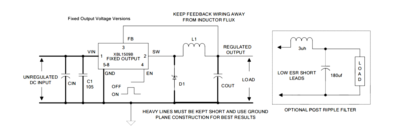
Simple circuit with few external components, suited for space‑constrained applications requiring tight output‑voltage accuracy.
2. Adjustable‑output mode (ADJ)
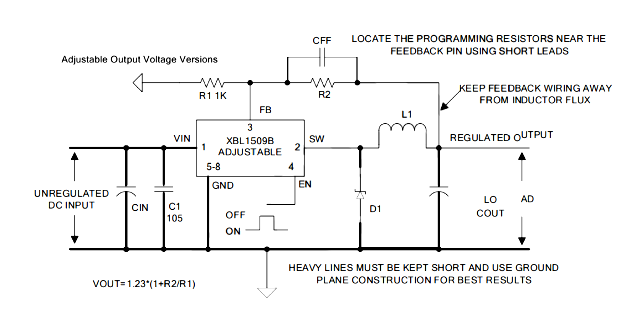
Output voltage is set by external divider resistors R1, R2. Offers high flexibility for non‑standard output‑voltage requirements.
> Design Note: Keep EN pin low or floating to maintain active output state.
3. Key Peripheral‑Component Selection Guide
3.1 Feedback Resistor R1
1kΩ, 1% tolerance resistor is recommended to ensure stable output voltage and good line‑regulation performance.
3.2 Input Capacitor C1
Place close to VIN and GND pins for suppressing input‑side voltage noise and ripple.
3.3 Compensation Capacitor CFF (for ADJ output or high‑output‑voltage conditions)
- Usage condition: Output voltage >10V, or low‑ESR output capacitor (solid / tantalum capacitor)
- Capacitance range: 100pF ~ 33nF
- Formula: CFF = 1 / ( 31 × 1000 × R2 )
- Material recommendation: X7R / C0G ceramic, plastic‑film or mica capacitor. Avoid Z5U ceramic type (poor temperature‑voltage stability).
4. PCB Layout & Thermal‑Management Recommendations
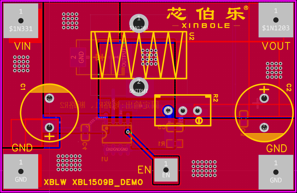
Proper layout is fundamental for stable power‑circuit operation:
- Feedback‑network routing: Locate FB pin and feedback resistors as close as possible. Use short direct traces and route away from switching nodes and high‑frequency noise sources.
- CFF placement: Must sit right beside feedback resistor R2 to prevent parasitic‑inductance effects.
- Thermal handling:
Under high‑load conditions, pour large ground copper area underneath IC body and add thermal vias for improved heat dissipation.
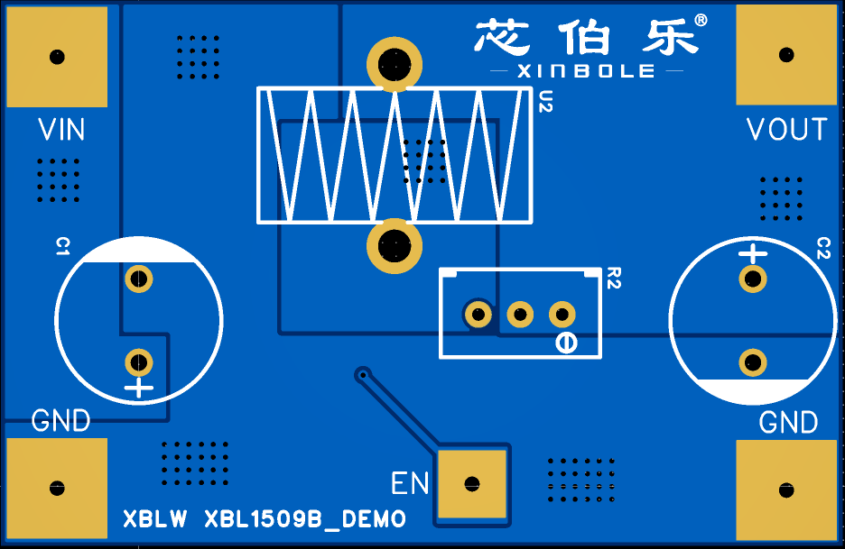
Single‑sided PCB is preferred for better electrical isolation and uniform thermal distribution.
5. Component‑Selection Reference Tables
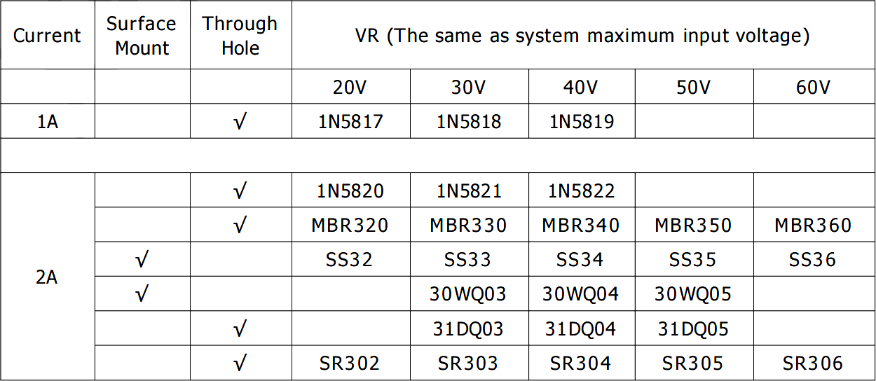
Schottky‑Diode Selection Table
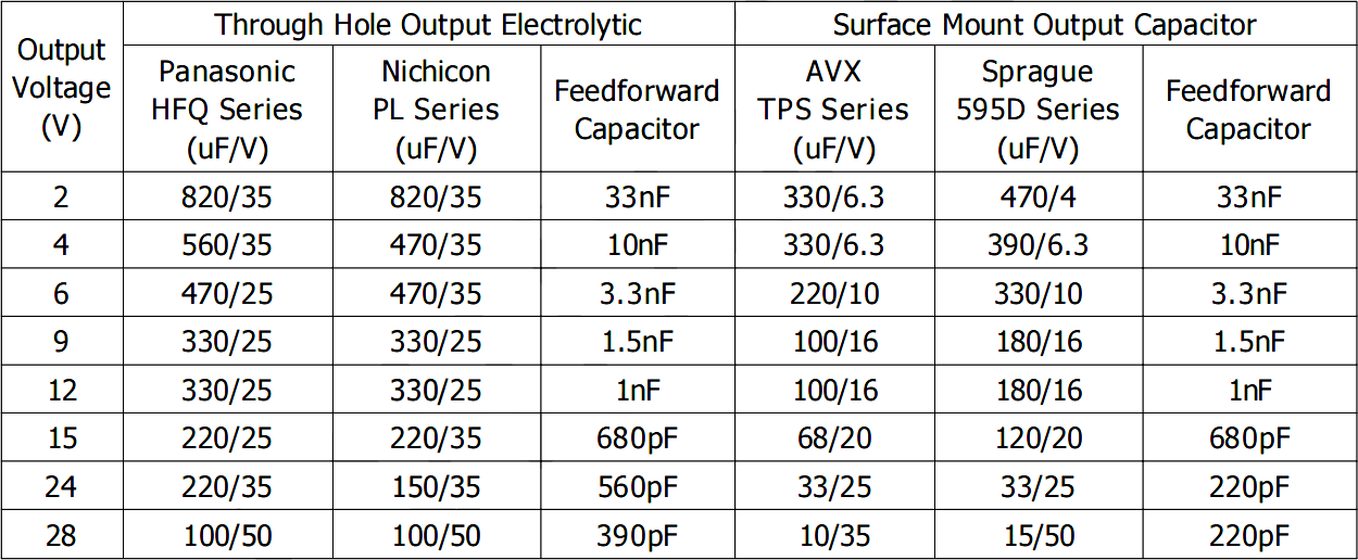
Capacitor‑Value Table (Adjustable‑Output Version)
Capacitor‑Value Table (Fixed‑Output Version)
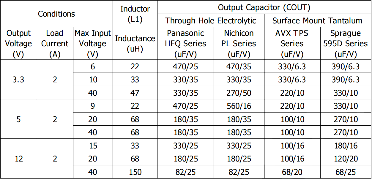
The above tables contain recommendations for Schottky diodes and input/output capacitors (fixed‑output / adjustable‑output). Engineers select parts according to real input‑output voltage, current rating and ambient‑temperature requirements.
6. Application Scenarios
XBL1509B is well‑suited for:
- Automotive‑electronic devices
- Industrial‑control & sensor power supplies
- Battery‑powered portable equipment
- Distributed power‑supply systems
- Compact‑form‑factor modules requiring high input‑voltage capability
Conclusion
With high efficiency, high integration and good load‑regulation performance, XBL1509B delivers a reliable step‑down power‑conversion solution. Proper circuit design, component selection and PCB layout further improve system stability and power‑supply quality. Evaluation demo boards are available to shorten customer verification cycles and accelerate time‑to‑market for end‑products.
Recommend News

Follow Us


-
Phone
400-9682 003