
PART 01
Chip Overview
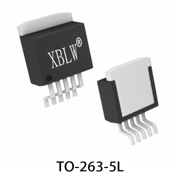
In the field of electronic circuit design, XBL6019, a chip launched by Xinbole, has garnered widespread attention for itsoutstandingperformanceandextensiverange of applications. The Xinbole XBL6019 is a monolithic integrated circuit specifically designed forboost,flyback, andforward converters. It integrates a 5A PMOSFET switch and essential protection circuits, with built-in features such ascurrent limiting,thermal shutdown, andundervoltage lockout, ensuring the circuit’sstable operationunder various operating conditions.
PART 02
Chip Features
1
Wide input voltage range
XBL6019supports3.6V~48Vwide input voltage range, adapting tovarious power supply scenarios, easily handling both battery-powered and industrial power environments.
2
High-efficiency conversion
Conversion efficiency reaches up to93%, thanks to the built-in optimized power MOSFETs and advanced circuit design, effectivelyreducing energy consumptionandheat dissipation requirements, thereby enhancing the device'sbattery lifeand operational efficiency.
3
Multiple protection features
On-chipthermal shutdown,current limiting, andundervoltage lockout—among other protection features—effectively prevent device damage caused byoverheating,overload, orabnormal input voltage,thereby enhancing system reliability.
4
Maximum continuous current output of 5A
Supportsup to 5A current output, providingstableandamplepower to a wide range ofhigh‑power loads, ensuring that devices always operate normally and do not fail due to insufficient power supply.
PART 03
Typical application scenarios
(1) Boost regulator
In applications such as LED lighting and charging portable devices, where low voltage needs to be stepped up to high voltage,XBL6019canefficientlyperform the voltage conversion task, providing astableoutput voltage.
(II) Flyback and Forward Converters
In switch-mode power supply design, the XBL6019 canimprovethe power supply'sconversion efficiencyandoutput stability, making it suitable for industrial power supplies and adapters, among other applications.
(3) Multi-Output Regulator
In complex systems requiring multiple output voltages, the XBL6019 can meet the power supply needs of different modules, simplifying the overallpower supply design。
PART 04
Typical Application Circuit
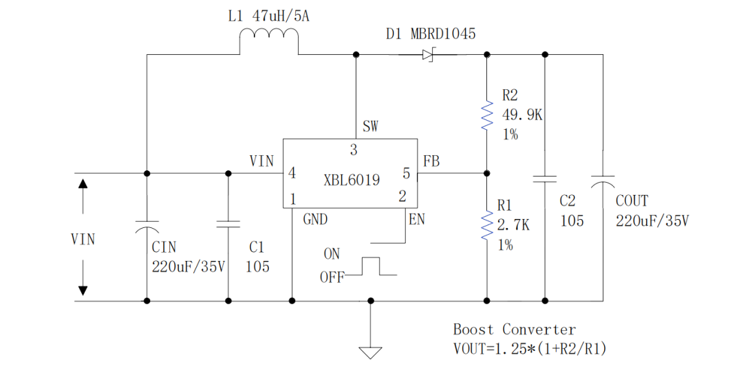
The figure above shows the typical circuit of the Xinbole XBL6019 boost converter. The input capacitor CIN and C1 are used to smooth the input voltage. The inductor L1 is controlled via the SW switching pin, enabling the boost function. The freewheeling diode D1 provides a freewheeling path when the inductor releases energy. The feedback resistors R1 and R2 form a voltage divider network to set the output voltage.Output capacitor C2COUT is used tosmooth the output voltage and reduce ripple, ensuring a stable power supply for theload.
PART 05
100W Output Power Dual-Channel Parallel Configuration
Inhigh-power application scenarios, theXBL6019 dual-channel parallel configurationcan achieve24V inputand100W output powerwith high efficiency. The circuit is shown in the figure:
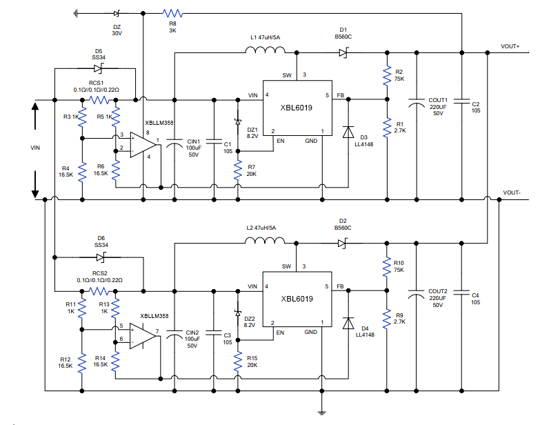
This circuit diagram shows a dual‑channel boost converter using theXBL6019 chip in a parallel configuration. By controlling the input current to limit the output power of each channel, it can meet a 24 V input and 100 W output requirement, while deliveringexcellent line regulationandload regulation. In this circuit, theinput current of each channel must be kept below2.5 A, and to ensure proper operation of theXBLW LM358op‑amp, its maximum supply voltage should not exceed 32 V. Additionally, the voltage difference between the op‑amp’s non‑inverting and inverting inputs must be at least 3 V lower than the supply voltage.Additionally, to preventinrush currentfrom damaging the sampling resistor, a Schottky diode should be connected in parallel across thesampling resistor.
PART 06
Application Cases and Precautions
(1) Application Cases

Large-scale energy storage products
When designinglarge-scale energy storage products,XBL6019canefficiently step up the inputlow-voltage DC powerto a higher voltage suitable for downstream circuits, whilemaintaining a stableoutput current, thereby meeting the downstream circuits’ requirements forstable power supply.

High-power portable power bank
High-power portable power bankrelies onXBL6019with a maximumoutput voltage of 60Vand a maximumoutput current of 5A, among other specifications, to ensurestable operation. Its highpowerand large currentalong with multiple protection featuresmake it widely used in the portable power‑bank sector.

Boost power supply module
The boost power supply module, with its wide input voltage range ofXBL6019 3.6V-48V and a maximum60V adjustable output voltage, can meet the power supply requirements of various downstream circuits. It also featureshigh conversion efficiency andovercurrent protection, effectively enhancing theperformance andreliability of the boost power supply module.
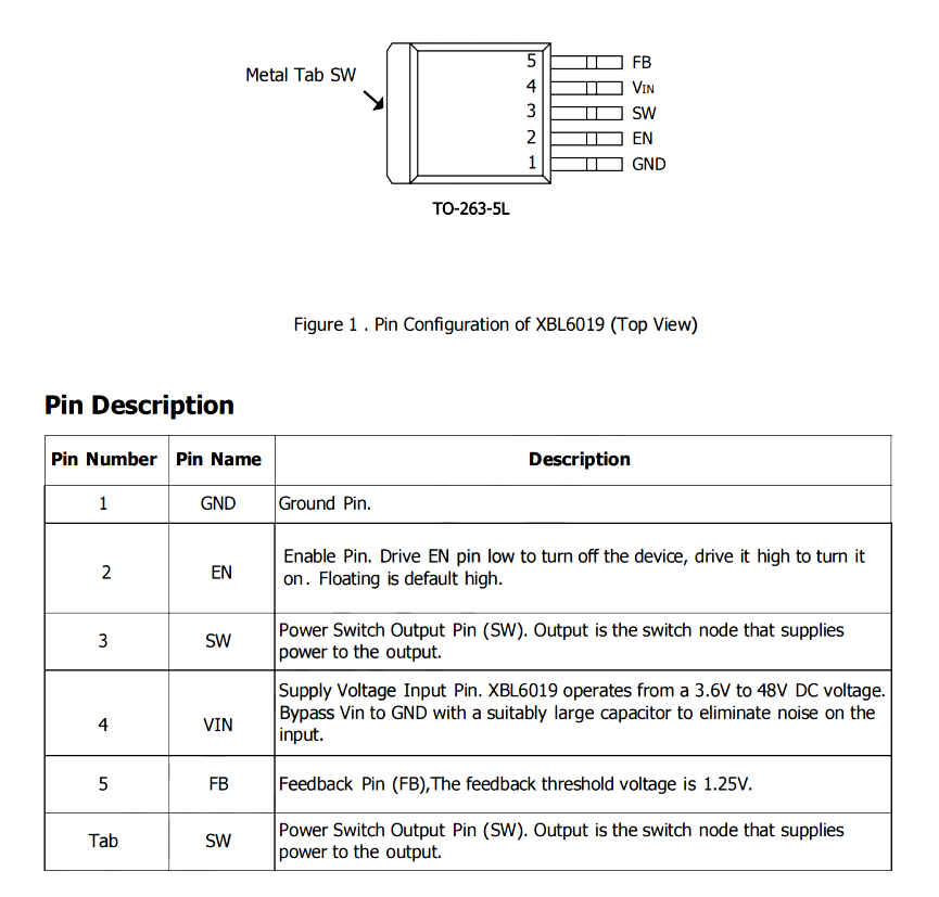
(II) Precautions
PART 07
Conclusion
XBL6019chip, with itsoutstanding performance andwide-ranging application versatility, offers electronic engineers anefficient and reliablepower management solution. Throughcareful design of applications, it canfully leverage its advantages across a variety of electronic devices. In practical use, engineers should, based on specific requirements and conditions, carefully consult the chip’s datasheet and adhere to relevant selection standards and guidelines to ensure thestable operation of the circuit and thereliable performance of the product.
Recommend News




Follow Us


-
Phone
400-9682 003