
XBLWSN74HC595DriverMOSFETDesignGuide
I. Overview
The XBLW SN 74HC595 is an 8 -bit serial input / parallel output shift register with a built-in tri-state output memory register . It is a commonly used I/O expansion chip in embedded systems , requiring only 3-4 I/O pins to expand 8 parallel outputs . It is widely used in LED control , digital tube driving , relay control and other scenarios.
This guide aims to help designers correctly usetheSN74HC595to drive MOSFETsand other devices, ensuring system stability and reliability.
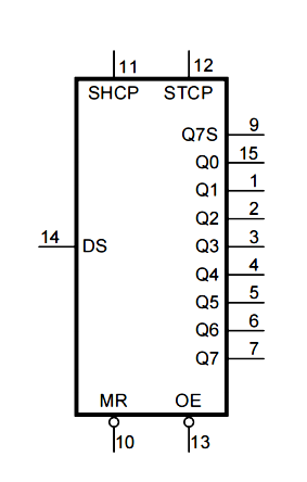
Logic symbol diagram
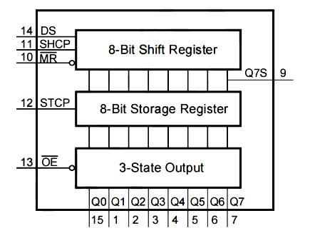
Functional diagram
II. Output Characteristic Analysis
According to the datasheet:
1.Output current capability
parameter | symbol | condition | Maximum value | |
Input clamping current | IiK | VI<-0.5V or VI>VCC+0.5V | ±20mA | |
Output clamping current | IandK | VO<-0.5V or VO>VCC+0.5V | ±20mA | |
Output current | IO | VO=-0.5V~(VCC+0.5V) | Q7S | ±25mA |
Q0~Q7 | ±35mA | |||
Power supply current | ICC | - | 70mA | |
Ground current | IGND | - | -70mA(Min) | |
Conclusion:The SN74HC595limitedoutput current capabilityand is recommended fordriving small-signal has MOSFETsor devices.
III.Pin Description
pin number | symbol | Function Description |
1 | Q1 | Parallel data output 1 |
2 | Q2 | Parallel data output 2 |
3 | Q3 | Parallel data output 3 |
4 | Q4 | Parallel data output 4 |
5 | Q5 | Parallel data output 5 |
6 | Q6 | Parallel data output 6 |
7 | Q7 | Parallel data output 7 |
8 | GND | power ground |
9 | Q7S | Serial data output (cascaded) |
10 | MR | Master reset (active low) |
11 | SHCP | Shift register clock (rising edge valid) |
12 | STCP | Storage register clock (rising edge valid, latched) |
13 | OE | Output enable (active low, high level indicates high output impedance) |
14 | DS | Serial data input |
15 | Q0 | Parallel data output0 |
16 | VCC | Positive power supply (2V~6V) |
IV.Typical Application Circuitsfor Driving MOSFETs
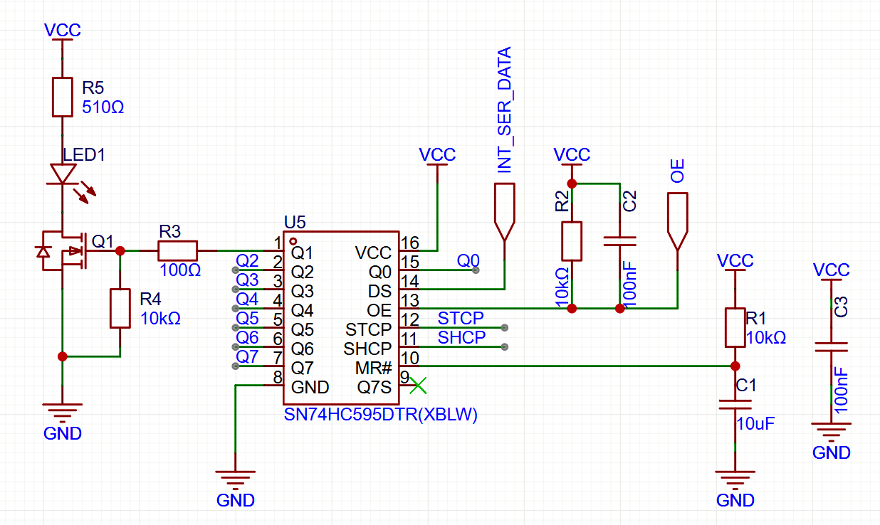
MOSFETl drive circuit
This part isthe execution layer of the circuit , which enables reliable on/off control of the LEDs :
1.Q1(N-channelMOSFET): Used asan electronic switch to control the on/ off state of the LED .
Drain: Connect to LED cathode; Source: Connect to GND ; Gate: Connect to QB ( pin 1) output of SN 74HC595 .
Work logic:
QBoutputs a high level→Q1gate receives a high voltage →MOSFETturns on→LEDcathode is pulled toGND→LEDlights up.
QBoutput low level→Q1gate pulled low →MOSFETcut off→LEDno current →LEDoff.
2. R3 (100 Ω gate resistor): suppresses gate oscillation during MOSFET switching and provides current limiting protection for the output pin of SN74HC595 , preventing high-frequency interference from damaging the chip or generating EMI .
3. R4 ( 10kΩ gate pull-down resistor): When the SN 74HC595 output is in a high impedance state (such as OE output disabled, power-on uninitialized), it reliably pulls the gate to GND , ensuring that Q1 is cut off and preventing the LED from lighting up falsely due to electrostatic discharge / interference .
Power supply and reset circuit
1.RCpower-on reset circuit (R1+C1):
Upon power-up,C1voltageis 0→MR#is low→SN74HC595shift register is cleared→ initial state.
All outputs are low ( LEDs are off); then C1 charges through R1 , MR# goes high , and the chip enters normal operation.
The statusis checked to ensure there are no abnormalities upon power-on.
2.OEstabilizing circuit (R2+C2):
OE is active low and requires a low enable output from the MCU. In the diagram, pull- up resistor R2 ensures that OE is connected to a high level during initialization to disable output , thus maintaining stability during the initialization phase .
3.Power supply decoupling:
C3 (100nF) serves as a power supply decoupling element , filtering out power supply noise during SN74HC595 operation and improving chip stability .
V.Typical Application Circuits for Driving Digital Tubes
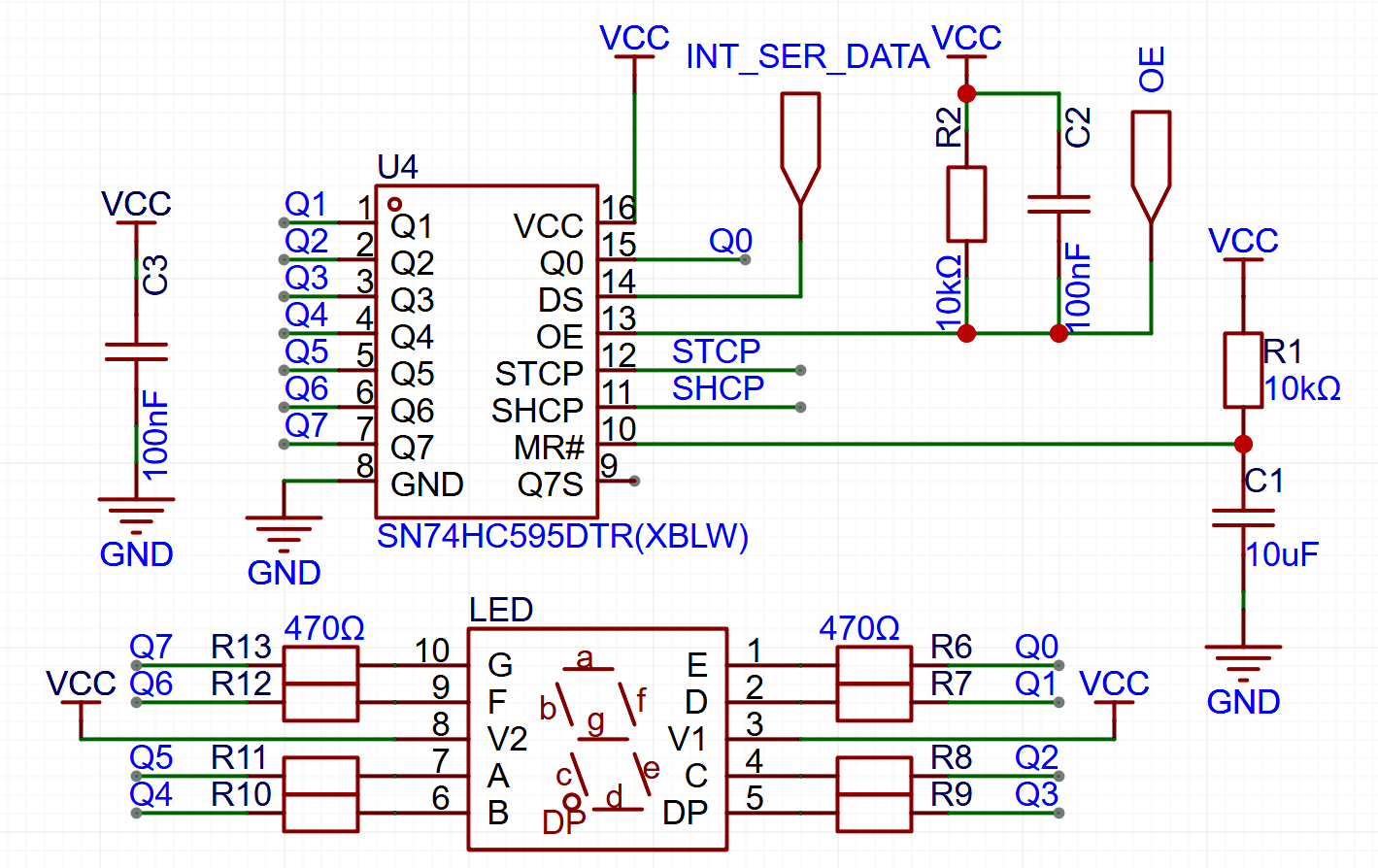
Digital tube driver circuit
This part is the execution layer of the circuit,wherethe XBLW SN74HC595implementsreliable on/off controlofthe digital tube:
1.A common anode digital tube,, with its common terminals (V1 is used V2, i.e., digit selection) directly connectedto VCC.Segment selection is controlled XBLWby SN74HC595 .
Working logic: The microcontroller outputs segment code data through the serial interface, which is converted into parallel output by the XBLW SN74HC595 to drive the corresponding segment of the digital tube (active low).
2.R6~R13arecurrent-limiting resistorswith a resistance of470Ω. If the forward voltage drop of the digital tube isVF=2VandVCC=5V, thenI=(VCC-VF)/R, meaninginput current to is approximately. It is recommendedthe XBLW SN74HC595 the 6.38mA,which is lower thanthe maximuminput sink currentto connect a separate current-limiting resistorfor each segment selectorto prevent uneven brightness .
Power supply and reset circuit
1.RCpower-on reset circuit (R1+C1):
Upon power-up,C1voltage is0→MR#is low→SN74HC595shift register is cleared→ initial state.
All outputs are low ( LEDs are off) ; then C1 charges through R1 , MR # goes high , and the chip enters normal operation.
The statusis checked to ensurethere are no abnormalities upon power-on.
2.OEstabilizing circuit (R2+C2):
OE is active low and requires a low enable output from the MCU. In the diagram, pull- up resistor R2 ensures that OE is connected during initialization.
A high input level disables the output, thus maintainingstability during the initialization phase .
3.Power supply decoupling:
C3 (100nF) serves as a power supply decoupling element , filtering out power supply noise during SN74HC595 operation and improving chip stability .
VI.Layout and Power Supply Recommendations
-The XBLWSN74HC595shouldbe placed as close as possible to the driven deviceto reducetrace inductance .
- Provide a 100nF decoupling capacitor for the XBLW SN74HC595 near the VCC pin .
High - power MOSFETs require a separate power ground to avoid grounding through the SN74HC595.
VII.Conclusion
The XBLW SN74HC595 , with its advantages of expanding eight parallel outputs using only three I /O ports , supporting cascading , and low cost , is widely used in scenarios such as digital tube displays , LED dot matrix displays , and button scanning . It has long-term prospects in resource-constrained embedded systems, educational practice , and low-cost control fields , and is a classic I/O expansion solution .
Recommend News

Follow Us


-
Phone
400-9682 003