
【Application】Wide‑Input‑Voltage & High‑Efficiency Regulation: XBL1509 DCDC Step‑Down Converter Design for Set‑Top‑Box Power Supplies
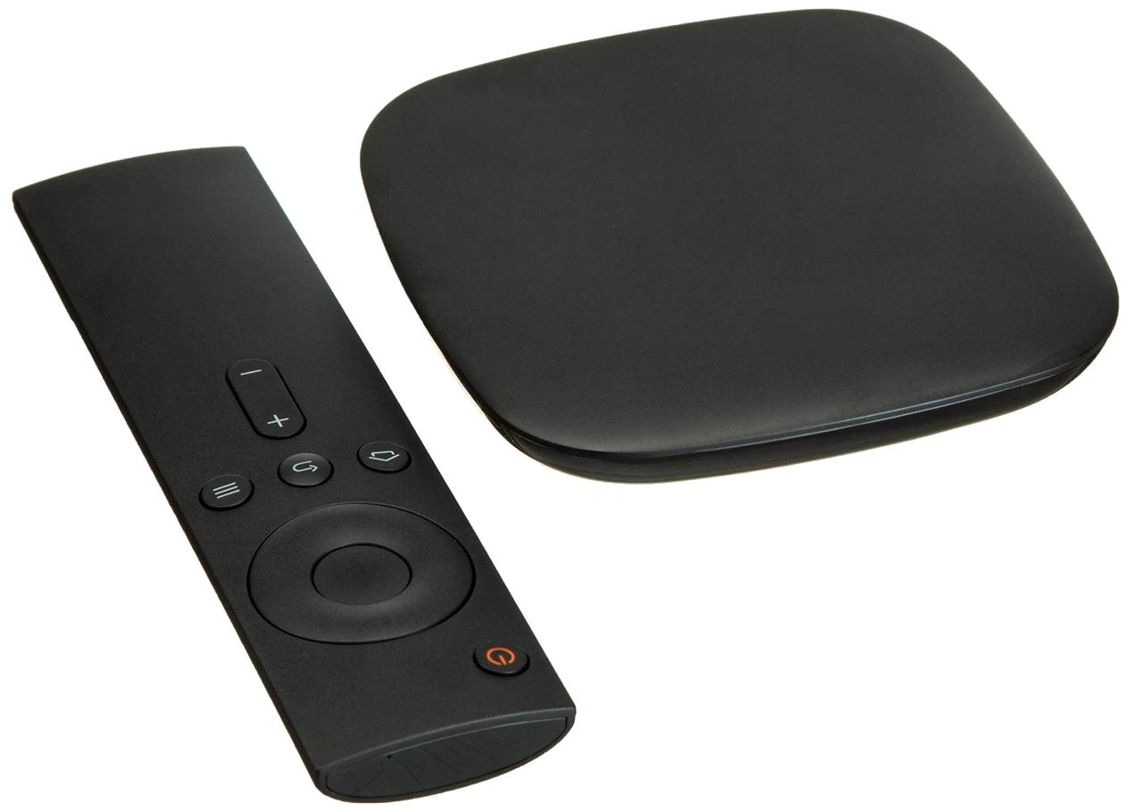
Inside the compact enclosure of modern set‑top boxes, an efficient and reliable power‑supply architecture is the foundation for stable operation. The XBL1509 is a classic 150kHz, 3A Buck DC/DC converter. Thanks to its wide input‑voltage range, high integration and straightforward design‑in process, it has become an ideal choice for many power‑supply engineers.
1. Chip Introduction: Meet Diverse Power‑Supply Requirements
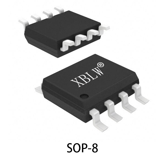
XBL1509 is a monolithic IC designed for step‑down DC/DC conversion. It can drive loads up to 3A without external power transistors, greatly saving PCB space. It features a logic‑level shutdown pin for low‑power standby mode. Its internal compensation network ensures good line and load regulation and simplifies external design. Fixed‑output (3.3V, 5V, 12V) and adjustable‑output (1.23V‑37V) versions are available in standard SOP‑8 or thermally‑enhanced ESOP‑8 packages.
2. Key Electrical Parameters
l Input‑voltage range: 4.5V to 40V. This ultra‑wide range supports multiple input sources including general‑purpose adapters from 4.5V~40V and delivers excellent power‑supply compatibility for set‑top‑box systems.
l Output voltage:
Adjustable (ADJ) version: Set via external resistors, range 1.23V to 37V.
Fixed versions: Available fixed rails: 3.3V, 5V, 12V. Output accuracy within ±4%.
l Output current: Continuous 3A, meets peak‑current requirements of mainstream set‑top boxes.
l Switching frequency: Fixed 150kHz. Compared with lower‑frequency ICs, it enables smaller‑size filter components (inductors, capacitors).
l Key electrical characteristics:
Feedback reference voltage (ADJ version): 1.23V (typical).
Efficiency: Excellent efficiency under typical operating conditions (up to 83% at 5V output), effectively reducing temperature rise.
Quiescent current: Typical value only 50µA under shutdown mode, supporting low standby‑power consumption.
3. Main Features & Advantages
1. High integration: On‑chip power switch delivers a complete step‑down solution with minimal peripheral components.
2. Comprehensive protection mechanisms:
Thermal shutdown: Prevents IC damage from over‑temperature conditions.
Current limiting: Limits switching current and provides overload protection.
3. Shutdown / standby control: Logic‑level control via EN pin. Input current is extremely low during shutdown, helping meet set‑top‑box energy‑efficiency standards.
4. Internal compensation: Simplifies design, no external compensation network required and guarantees stability across operating conditions.
4. Typical Application Scenarios in Set‑Top‑Box Systems
Inside set‑top‑box systems, XBL1509 can be flexibly used for devices requiring different supply voltages:
l Core voltage conversion: Efficiently steps down 12V adapter input to multiple secondary voltages required by downstream devices.
l System voltage generation: Directly produces 3.3V or 5.0V (fixed versions), supplying clean power for front‑end LDOs of DDR memory, Flash and other peripherals.
l Secondary step‑down input: If primary pre‑regulation already exists, XBL1509 performs secondary high‑efficiency buck conversion to deliver independent, clean power to different loads.
5. Application Solution & Circuit Design Guidelines
Set‑top‑box power‑supply schematic:
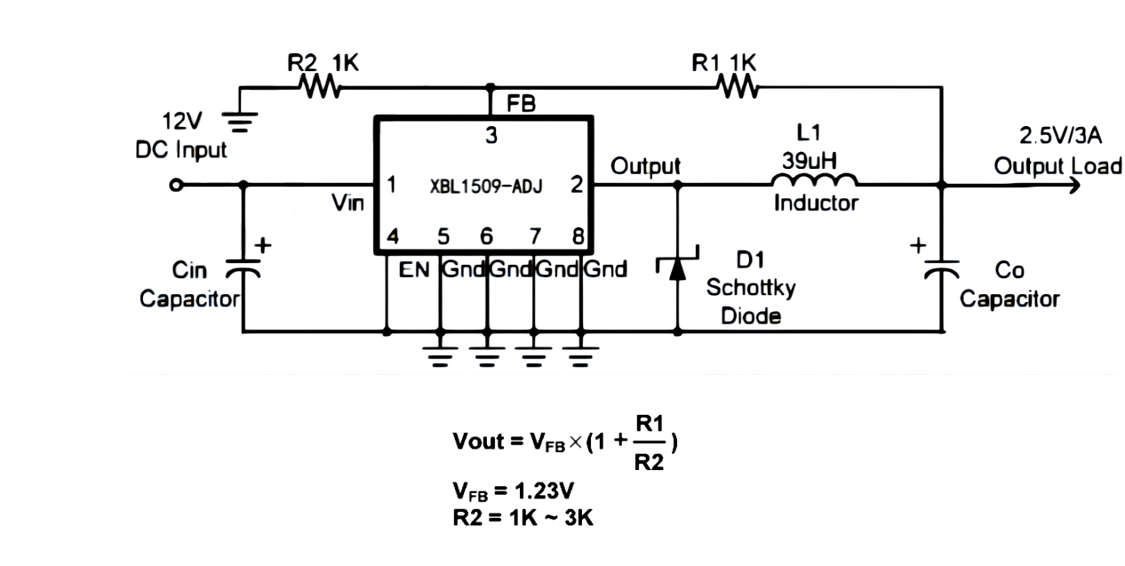
Design Notes & Key‑Component Selection:
1. Inductor (L1):
Selection criteria: Choose based on input voltage, output voltage and load current. Recommended 47µH for 40V‑in / 3.3V‑out /3A; recommended 68µH for 20V‑in /5V‑out /3A.
Key parameters: Saturation current must exceed IC peak current‑limit value; rated RMS current shall be larger than maximum output current.
2. Output capacitor (Cout):
Function: Filtering and providing load transient current.
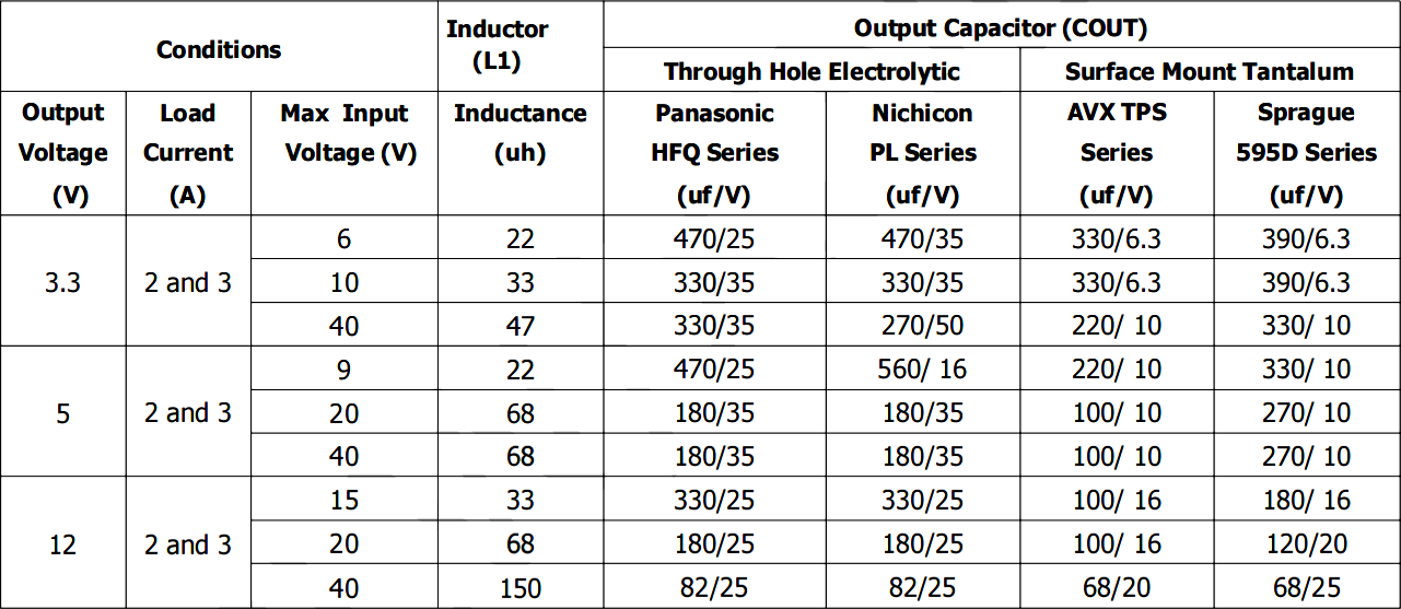
Example: For 3.3V output, 330µF/35V electrolytic or 220µF/10V SMD tantalum capacitor is recommended. Refer to below figure for values of other output‑voltage / current combinations.
3. Freewheeling diode (D1):
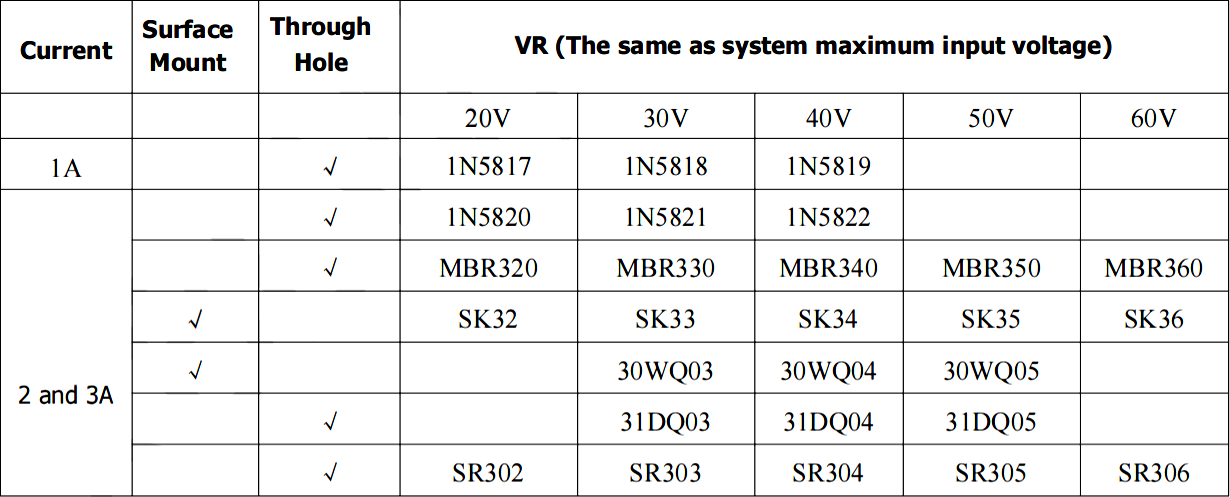
Selection: Must use fast‑recovery or Schottky diode. For 1A: 1N5819 (40V); for 3A: SK34 / SR304 (40V). Reverse withstand voltage shall be no less than maximum input voltage.
4. Enable & delayed start‑up:
l EN pin can implement power‑on sequencing with simple RC network to avoid multi‑rail power‑on surge. Tie EN pin directly to ground if shutdown function is not required.
l PCB Layout & Thermal Management Notes (critical):
Thermal design: XBL1509 requires good heat dissipation under heavy‑load conditions. The exposed pad must be fully soldered to PCB copper area and connected via multiple vias to inner‑layer or back‑side large ground / thermal copper plane, which is key for low thermal resistance.
l Noise isolation: FB feedback trace shall be routed away from inductors and diodes (noise sources) and directly tap at feedback‑resistor nodes. Constrain copper area of switching‑node (Output pin) to minimize radiated emission.
6. Summary
With 40V wide‑input capability, 3A continuous output, high‑integration and classic fixed‑frequency PWM control architecture, XBL1509 delivers strong practical performance and reliability for set‑top‑box power‑supply designs. Multi‑variant output‑voltage options bring design flexibility, while comprehensive protection features plus low standby current guarantee system safety and energy‑saving performance.
Recommend News

Follow Us


-
Phone
400-9682 003